In this article, we are going to discuss PCB and PCBA. PCB and PCBA are two essential aspects of electronic circuit boards, which provide the functionality to printed circuit boards.
Generally speaking, PCB is for signal processing and power supply, while PCBA is for assembling components into a finished product.
If you want to learn more about PCB and PCBA, first you should learn the basics of PCB and PCBA. We’ll talk about them in detail below.
PCB VS PCBA: What is the difference?
What is PCB?
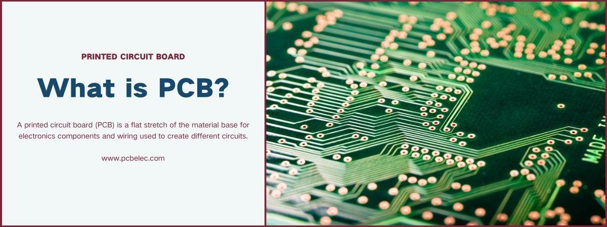
A printed circuit board is a flat stretch of the material base for electronics components and wiring used to create different circuits. PCBs are often made from fiberglass or metal sheets laminated with copper shapes forming the circuits.
Further Reading
- Classification Of PCB Materials And How To Choose The Correct PCB Substrate
- What Is FR-4 Material In PCB Fabrication?
- Why choose FR4 as the general material of PCB?
- Unveil the mystery of high TG PCB circuit boards Materials
- What is the Tg value of PCB substrate?
- Complete Introduction of Flexible Circuit Board Materials
The components and wires can be attached to the surface of the PCB by solder & then the entire PCB can be covered with a protective coating (The protective coating, which means the solder mask, can be white, red, blue, green, etc. Green is the most common PCB color.).
PCBs are created through a process of photolithography, which is a method that uses light to transfer a pattern from a mask to a light-sensitive chemical layer on the surface of PCB. The pattern then can be etched into the copper layer.
Then, electronic components are attached to the PCB with solder, and wires are connected through a process called reflow soldering.
The coating is applied to protect the PCB from corrosion or outside damage at the end of this process.
Depending on their function, PCBs may be made in a variety of forms and sizes. They can be designed flat for insertion into a printed circuit board enclosure, or they can be designed with mountings and connectors to allow them to be connected to other devices.
What is PCBA?
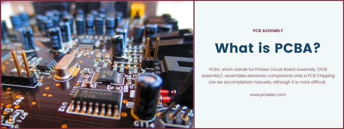
PCBA, which stands for Printed Circuit Board Assembly (PCB Assembly), assembles electronic components onto a PCB Chipping can be accomplished manually, although it is more difficult. This might include as little as mounting and soldering chips, resistors, capacitors, and other discrete components. It may also involve attaching leads to ICs or inserting pre-made connectors.
The finished product is subsequently inspected for any flaws. If it passes inspection, the PCBA may be covered with epoxy or laminate for additional protection and to improve its durability.
Board stuffing is the initial step in the assembly process. You take your blank PCB and solder down components one by one for this stage.
Soldering each lead on a chip to a PCB is the next step.
After that, it’s time for any surface mount components to be placed and soldered down. For this step, machines with computerized vision systems are used. They can identify and pick up tiny parts much smaller than a grain of rice and place them into position with precision accuracy using solder paste.
This completes the main body of the PCB. However, there are still a few things to accomplish.
First, any through-hole components need to be inserted into their designated spots and soldered in place.
Then, the board needs to be cleaned up. Any excess solder, flux, or other materials must be removed so that the board looks neat and professional.
Finally, the board must be checked for functionality. Any mistakes must be corrected before the PCB can be considered finished.
The placement of the PCBA on the board is a complicated operation that requires a substantial amount of expertise and accuracy.
However, it is also one of the most important phases in the process of creating a functional electronic device.
Further Reading
JHYPCB provides one-stop through-hole PCB assembly, SMT PCB assembly, prototype PCB assembly, LED PCB assembly, and low volume PCB assembly services.
What are the different types of PCB?
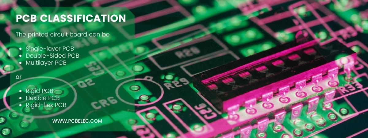
All electronics are divided into two broad categories: printed circuit boards and etched circuit boards. Here we will talk about Printed Circuit Boards or PCBs. The printed circuit board can be single-sided, double-sided, or multilayer, and it can also be rigid PCB, flexible PCB, or rigid-flex PCB. The insulating substance between the layers of PCBs is usually a dielectric.
For more knowledge about PCB classification, please click here to learn more.
A single-sided printed circuit board is used for prototyping and low-reliability applications. The top foil or layer has all the components and the conductive pattern on the other side. These boards are made from one side of a sheet of 1/16-inch-thick fiberglass-epoxy, with the copper foil laminated onto the surface.
The main advantage of single-sided boards is that they are quick to produce and require few manufacturing steps, thus keeping costs down. However, the disadvantage is that this method does not allow for high-density designs due to difficulty routing the signals between two different layers. The conductive pattern can also be subject to electromagnetic interference (EMI).
Designers often use single-sided boards when they are in a hurry, need to keep costs down, prototype high volume designs, or do not require multi-layer boards. Single-sided PCBs are also used for low-powered and low-frequency devices.
A double-sided printed circuit board has two layers, each with its own conductive pattern and components. The top layer has the components, and the bottom layer has the conductive pattern. The two layers are frequently separated by a dielectric, which is an insulating substance. This type of board is quicker to produce than a multi-layered board and is more expensive than a single-sided board.
Double-sided PCBs are used for medium power and frequency devices. The two sides of the board offer better performance than a single-sided board due to the increased density that can be achieved. The two layers also make routing signals between components much more accessible.
A multi-layered PCB has more than two layers and is used for high power and high-frequency devices. Number of layers in a PCB is limited by the thickness of the board and the manufacturing technology used. Multi-layered PCBs offer better performance than single or double-sided boards due to the increased density that can be achieved.
Multi-layered PCBs are normally used in high-end electronic equipment where performance is key and price is no object. A multi-layer board requires more manufacturing steps than a single or double-sided board, and each additional layer increases cost. The use of vias also produces additional expense as these holes need to be accurately drilled and plated.
A multi-layer PCB may consist of many different layers, some of which may include:
Power planes or power traces (conductive material on a coating that provides a common path for electrical currents),
Ground planes (a completely connected conducting surface on one or more layers; intended to give an unbroken conducting way for relatively low-current signals and to enhance the ground-referenced noise performance),
Signal planes (conducting material on a layer that provides a common path for relatively high-frequency or fast electronic signals).
Further Reading
This is sometimes referred to as an HDI (High-Density Interconnect) PCB. The main differences between this type of board and a standard PCB are:
HDI boards feature blind and buried vias. A via is a hole that connects two board layers together, but does not go all the way through as drilled holes do. Instead, they stop at the first inner layer. This leaves no visible trace on the board’s surface for either coating. This configuration allows more components to be placed on a board and allows for shorter, faster paths for electrical signals.
HDI boards also have microvias. A microvia is a tiny via, typically less than 0.0039 inches in diameter (0.1mm). They are used to connect the very most minor components to the board. These may not be possible with the standard size of 0.0138 inches (0.35mm).
Recommened Post: HDI PCB Layout and Basic HDI Design Guidelines
What Is the Difference Between PCB and PCBA?
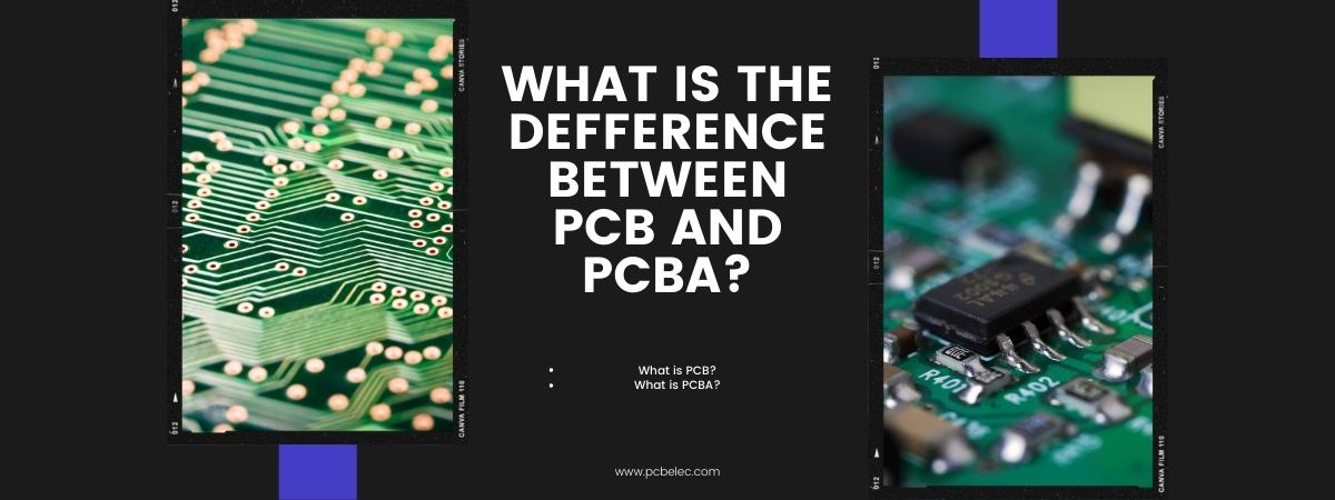
There are a few critical differences between PCBs and PCBA. The first is that PCBs are just the boards, while PCBA includes the electronic components soldered to the board. This means that a PCB can be used for various projects, while a PCBA is specifically designed for a particular project.
Another difference is that PCBs are typically cheaper to produce, while PCBA’s tend to be more expensive. This is because the process of soldering the electronic components to the board is more complex and time-consuming.
Finally, PCBs are not as reliable as PCBA’s. This is because a PCB relies on the electronic components to function correctly, while a PCBA has the electronic components built into the board. This makes them more reliable and less likely to fail.
So, which one should you choose?
Choose a PCB if you want the cheapest and simplest approach. If you require a more dependable and durable option, go with PCBA.
Where are PCBs used?
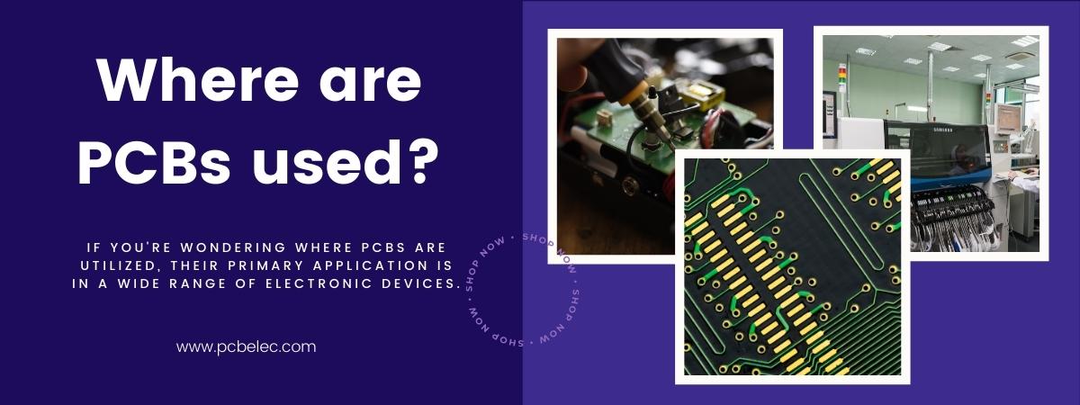
If you’re wondering where PCBs are utilized, their primary application is in a wide range of electronic devices. Mobile phones, televisions, and cameras are just a few examples. Printed circuit boards in automobiles, medicine, computers, and other applications are common practice.
Power amplifiers are used to produce graphics cards and motherboards, among other things. The printed circuit board has a broad range of uses in various sectors because it transports electronic components and connects them, regardless of the type of equipment involved. The wiring is straightforward and compact, allowing for the manufacture of tiny gadgets without difficulty.
In today’s technological society, where technology has developed significantly, PCBs are integrated into the circuitry and switch for different circuit elements. They’re also used to help regulate how electricity travels from one part of the construct to another so that it doesn’t cause problems when too much power is applied to a single area.
What are the advantages of PCB?
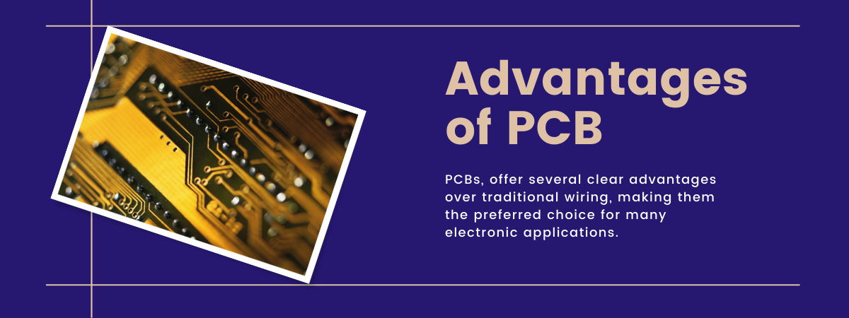
PCBs are known to have many advantages over traditional wiring. Some of these advantages include:
- Increased space savings – PCBs can be designed to take up much less space than traditional wiring, freeing up valuable room in crowded electronic assemblies.
- Faster assembly – PCBs can be assembled much faster and more efficiently than traditional wiring, leading to reduced manufacturing times and costs.
- Increased reliability – PCBs are much more reliable than traditional wiring, which can often be susceptible to failure caused by wear and tear.
- Easier maintenance – PCBs can be easily maintained and repaired, whereas traditional wiring can be difficult and time-consuming to work with.
- Lower manufacturing costs – PCBs are cheaper to produce than traditional wiring due in large part to their increased reliability and ease of assembly.
- Design flexibility – PCBs can be designed for nearly any application, whereas traditional wiring is limited by the physical connections required at each point between components.
- Increased safety – PCBs are less likely to cause electrical fires or other safety hazards than traditional wiring.
Overall, PCBs offer a number of clear advantages over traditional wiring, making them the preferred choice for many electronic applications. PCBs are becoming an increasingly popular choice for manufacturers and consumers alike thanks to their space-saving design, fast assembly, and increased reliability. For these reasons, PCBs will likely continue to play a dominant role in the electronics industry for many years to come.
What are the benefits of PCBA Technology?
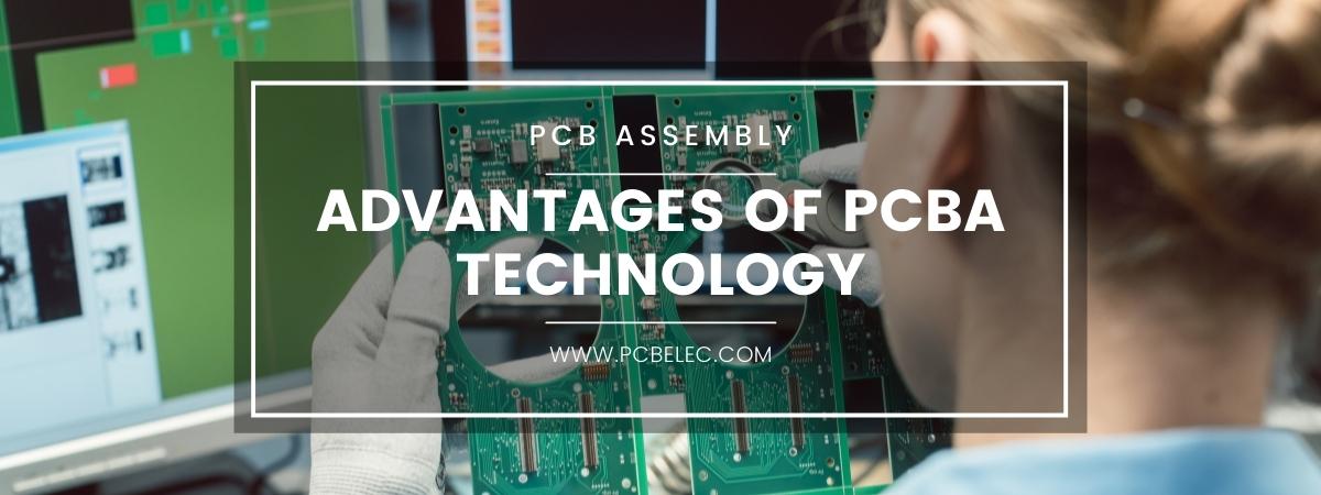
PCBA is an acronym for printed circuit boards assembly. It is a process where circuit boards are assembled. This means components, such as resistors, capacitors, and integrated circuits (ICs), are soldered to the copper lines on both sides of the board. These components are then protected with a cover.
The popularity of PCBA technology is due to the many advantages it offers. These advantages include:
- Reduced manufacturing time and costs –PCBA technology allows for the assembly of complex boards in a fraction of the time it would take using traditional methods. In addition, less labor is required, which results in lower costs.
- Improved quality – The components used in PCBA are manufactured using the latest technologies and industry standards. These methods help ensure that all components go through careful testing to meet high-quality standards. If any defect is found, these parts will not be sold to customers or suppliers until repaired.
- Improved manpower management –The use of PCBA technology allows companies to hire fewer workers. This is because manual tasks involved in assembling the boards, such as placing components and soldering, are automated. For instance, there would be no need for people to sit down and solder one element at a time. They can instead work on higher-value tasks.
Disadvantages of Printed Circuit Boards
There are a few disadvantages of PCBs that should be considered before deciding to use them in a design. The first is their cost; PCBs can be expensive to produce, incredibly complex ones. This can be a significant drawback for smaller companies or individuals who don’t have the budget to invest in this technology.
It’s a time-consuming procedure that takes hours, if not days, to finish. Also, the solder mask and silkscreen on a PCB must be perfect, or else it may affect how components connect, which can lead to some rework. This also goes for the patterned copper layer on the board as well. A small error in the pattern can cause a significant effect on if the board works as intended.
Another downside to PCBs is their fragility. They can easily be damaged if not handled with care, and they are susceptible to environmental conditions such as temperature and humidity. This can cause problems during the manufacturing process and may even lead to products not working correctly in the field.
A PCB also has some mechanical limitations, such as rigidity and weight. Since a PCB is made of FR4 material, it is somewhat flexible and heavy. This can be a pain if you want to use them on a lightweight device.
Finally, PCBs are not always recyclable, making disposal of them a problem in some situations.
Disadvantages of PCBA
The disadvantages of PCBA (printed circuit boards assembly) are listed as follows
- Cost-PCBA is a complex process involving many techniques and equipment, including baseboard materials, patterns, surface finishes, components, and assembly. Cost Increases as a Result of All of These Reasons.
- Time-PCBA assembly can be time-consuming, as each step must be completed accurately and in the correct order to avoid damaging components or boards. This can lead to longer lead times for products.
- Versatility-PCBA is not as versatile as other methods of board assembly, such as through-hole. This can limit the types of products that can be manufactured using PCBA.
- Quality- Due to the complexity of the procedure, PCBA assembly quality is sometimes inconsistent. Incorrect assembly or component placement can lead to products that do not function correctly or that are unreliable.
- Environmental Impact-The use of chemicals, fluxes, and other materials in the PCBA process can have a negative environmental impact. This must be considered when choosing this method of the board assembly.
PCBA is a complex process that has several disadvantages. Increased production costs, longer lead times, and less versatility are just a few of the potential problems with PCBA. Before selecting this sort of board assembly, it’s vital to consider all of the variables.
What is the PCB manufacturing process?
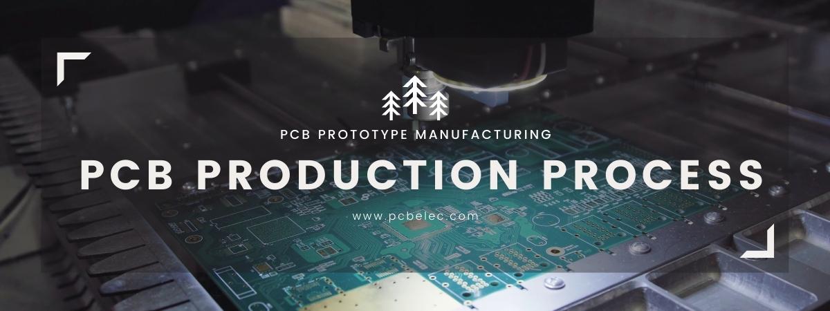
This is a lengthy procedure with many stages. It’s all about manufacturing stuff in a factory. This is a lengthy procedure with many stages. Let’s take a look at them one by one.
The first step is to make the copper foil. This is done by casting copper into a thin sheet. The sheet is then cut and rolled out into a long piece. It’s then cut again into smaller pieces about the size of a PCB.
Next, the photo-resist is applied to the copper foil. This helps in etching away the copper in certain areas. This is done by exposing the foil to light through a photomask. This makes it possible for an exposure device to transfer all of this information onto the foil, so when it’s submerged in water, only parts of the foil are eaten away while other parts remain intact. It’s then washed away with water, leaving holes that are shaped according to the photomask.
Next, a wet sanding process is done on the foil. This gives it its final smoothness before the etching process begins.
This step is where the copper layer is etched away by acid. Areas not protected by the photo-resist are removed, leaving behind only the parts of the copper which were needed. This process is done using acids instead of any other solution because it will eat away just about any metal except gold or silver. After this process is complete, all that’s left are the copper tracks and pads that will be used to create connections between components.
Next, a thin solder coating is applied to the entire board, which acts as a barrier to prevent oxidation when gold or nickel is deposited.
The next step involves depositing gold alloy on the top side and nickel alloy on the bottom side of the board. This is done to prevent oxidization and make the board look good.
The last step is to drill all of the holes needed for the screws and other components. The board is then ready for use!
Further Reading
Component of PCBA
PCBAs are a component of many portable electronic devices. They consist of a small fiberglass-like material containing a patterned metal layer used to connect all the other parts. The components, such as the integrated circuits and transistors, are attached to this board with tiny metal beads called “solder balls.”
The solder balls are then heated until they melt, forming a permanent bond between the components and the board. The PCBAs are then enclosed in a plastic or metal case to protect them from the environment.
The components attached to the board usually include integrated circuits and transistors. A few examples of common integrated circuits include:
- Analog-to-digital converters.
- Digital-to-analog converters.
- Microprocessors.
- Central processing units.


