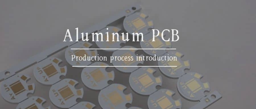
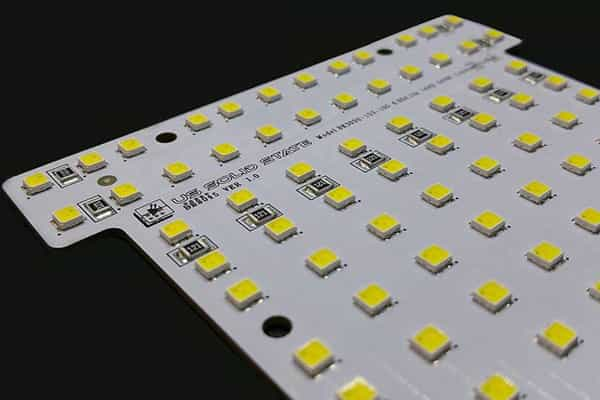
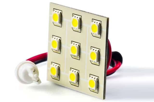
What is aluminum PCB?
An aluminum PCB is a printed circuit board that contains a thin layer of conductive dielectric material. They are also called aluminum cladding, aluminum base, MCPCB (metal clad printed circuit board), IMS (insulated metal substrate), thermal conductive PCB, etc. Aluminum PCBs were developed in the 1970s, and soon their applications increased sharply. The first application is their use in amplifying hybrid integrated circuits. They are being used on a large scale, so we must understand aluminum PCB and its importance.
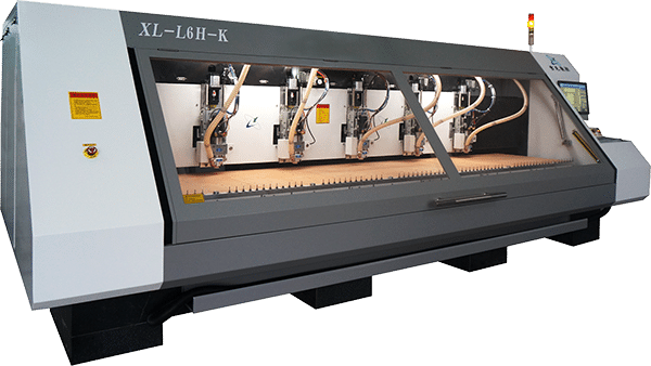
The aluminum PCB manufacturing process
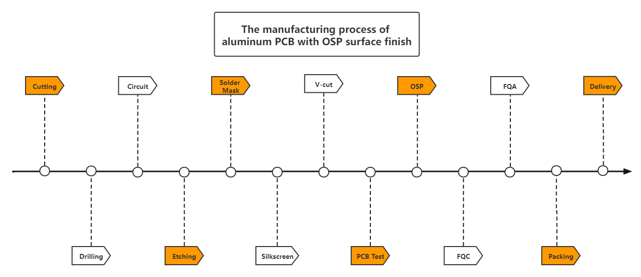
The manufacturing process of aluminum PCB with OSP surface finish: Cutting→Drilling→Circuit→Acid/alkaline etching→Solder Mask→Silkscreen→V-cut→PCB Test→OSP→FQC→FQA→Packing→Delivery.
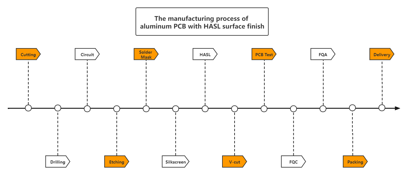
The manufacturing process of aluminum PCB with HASL surface finish: Cutting→Drilling→Circuit→Acid/alkaline etching→Solder Mask→Silkscreen→HASL→V-cut→PCB Test→FQC→FQA→Packing→Delivery.
JHYPCB can provide the aluminum core PCB with the same surface finish process as FR-4 PCB: Immersion Gold / thin / silver, OSP, etc.
Detailed internal process of aluminum PCB manufacturer
Step 1. IQC
- Cu surface check: Notches, scratches, and severe oxidation are not allowed.
- Protective film check: Protective film mustn’t be broken with Cu exposure.
- Thickness check: Checkboard thickness and Cu thickness according to the lot card.
Step 2. One-time Hole-punching/drilling
- One-time hole-punching/drilling is mainly to punch orientation-hole and technical hole. The hole position and hole diameter must be consistent with the drawing requirement.
- Punching/drilling direction is from Cu surface to AI surface, effectively avoiding scratches of AI surface.
Step 3. Image Transfer
3.1 Scrubbing
- A. To improve the combination of dry film & protective film and avoid falling off-dry film on the protective film, it is necessary to scrub the surface of protective film lightly.
- Oxidation and left glue stains on the board surface cannot be allowed.
3.2 Film
- The interval between pre-cure and film-pasting time should be as short as possible.
- Placing and Cooling
To assure accurate registration, it is necessary to place an aluminous board with pasted film for a while until it reaches room temperature.
- Negative Yellow Film. Pay attention to be registration accuracy of the silkscreening hole.
- Placing
The light-gathering reaction happens at the circuit part and reaches complete aggregation after 15 minutes.
- Developing
Step 4. Image Check
- Mainly check open circuit, short circuit, gap and unclean developing, etc.
- Black oil-pen cannot be used when mending board but black oil.
Step 5. Etching
- It is obligatory to conduct mass production after the first batch of boards is confirmed to be qualified.
- The dilapidation of the protective film is not allowed, and if the protective film is broken, it should use adhesive tape to mend it before placing boards on the etching machine.
- Assure one-time clean etching as possible it can.
- Using a knife to scrape off left Cu on any part of the pattern or the dirt on the insulating layer is not allowed.
Step 6. Film-stripping/Cleaning
- To strip the films clearly, use a tackle roller instead of immersing in the stripping chemistry.
- The residues of the stripping chemistry would affect the durability of the IMS, so it needs efficient cleaning after stripping films.
- Baking is required after stripping.
- No manual etching is allowed.
- If etching was not well done, re-fetch is needed quickly.
Step 7. Etching Check
- Using a knife to scratch any part of the insulating layer is not allowed.
- Mainly check short circuit, gap, open circuit. The vacant unit mustn’t be drilled and marked with “x” by a black oil pen.
Step 8. Solder Mask Making
- Single-side scrubbing(circuit side). Oxidation and glue stains on the board surface are not allowed.
- Print solder mask after the boards is cooled to room temperature.
- Register and expose aluminum PCB after it is cooled to room temperature.
Before registration, it is necessary to check if the sensitization oil accumulates on the board surface or is uneven. If there is a lot of sensitization oil on the board surface, it must re-process such boards in time.
During registration, it is necessary to pay attention to the concentricity of the film and mark point.
- Exposing
- Developing
- Check: Mainly check unclean developing and solder mask on the PAD.
- It must rip off the protective film on the AI surface after developing for unspecialized boards. Glue stains and protective film leftover on the AI surface are not allowed.
Remark: If the customer has unique requirements, the protective film mustn’t be ripped off after developing, even during the whole production.
- The protective film cannot be ripped off before washing off the solder mask for re-process and should be checked if it is broken. If the protective film is broken, it must be mended with adhesive tape.
Step 9. Orientation-hole Punching
- Punch orientation-hole at the corresponding position of the board with finished circuits by layer pressing punching.
Step 10. Component Mark Making(Based on the requirement of MI)
- Conduct self-check for every printed working board and continue printing when the previous one is qualified. Unqualified boards must be separated from qualified ones and be re-processed in time.
- Component mark mustn’t be ambiguous, broken, oil seeped or with ghost image.
Step 11. HALS
- The Tin-oven temperature is controlled within XXX℃.
- Conduct post-treating when the board is thoroughly cooled after HALS.
- Completely clean the board surface at the hot-water washing section of the post-treating to avoid the dim colour of the board surface.
Step 12. HALS Check
- The Tin surface must be smooth without Tin-piling and high Tin.
- Assure all solder points are covered with Tin.
- All mark points must be smooth. It is not allowed that the Tin surface to be protruded or uneven.
- The colour of Tin surface must be unified with good brightness and no dim colour.
Step 13. Single-side Scrubbing (according to customer’s requirements)
- Completely clean the machine and change dirty water before scrubbing, and there must be ****
- Using felt tackle for scrubbing. The type of former scrubbing brush is ***, and the latter is**. The tested width of the scrubbing trace is within**mm.
- Pay attention to cleaning transporting tackle at the baking section before scrubbing.
- Use a pair of upper scrubbing brushes for scrubbing. Put the circuit side adown and turn off the nether scrubbing brush.
- If there are scratches on the Al surface, it is necessary to use ***** sandpaper to smooth the board and then conduct scrubbing.
- The Tin surface mustn’t be polluted and shouldn’t have dim colour.
- All parts of the AI surface must be scrubbed evenly.
- Paste particular colourless protective film on the Al surface after the Al and Tin surfaces are qualified.
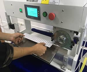
Step 14. V-cut
- Apply computer-assistant v-cut.
- During v-cut, it mustn’t rip off or uncover the gummed paper and touch the AI surface by hand.
Step 15. Moulding
- During the whole production, it mustn’t rip off or uncover the gummed paper and touch the AI surface by hand.
- The punching & pressing direction is from a circuit side surface to AI.
- There mustn’t be apparent burs on the AI surface
- The board mustn’t be broken when pressing, and the circuit side mustn’t be polluted.
- The insulated layer mustn’t be fallen off.
- The tolerance of outline and controlling position should be consistent with design requirements.
- Pay attention to cleaning the upper and nether moulds during punching & pressing for any metal crumb that may damage the insulating layer and influence the electrical capacity of PCB.
Step 16. High-pressure Test
- To assure sufficient insulated intensity for the aluminous PCB, the high-pressure test must be operated according to the customer’s requirements.
- The pressure of the high-pressure test is ****KV DC, and the creepage current is**mA/PCS.
- If there is creepage of high-pressure tests, it must test board one by one to find out the creepage unit.
- Testers must wear insulated rubber overshoes and insulated gloves to avoid electrical hurt.
Step 17. OSP
- The OSP film thickness must be in the required scope.
- The OSP film should be even.
- The colour of the AI surface cannot be changed, and the AI surface mustn’t be scratched.
Step 18. FQC and FQA Check
- Check the board according to the combination of aluminous PCB standards below and customer standards.
- Uncover the gummed paper on the Al surface during checking and separate the boards with white paper.
- The AI surface and circuit side cannot be polluted during checking.
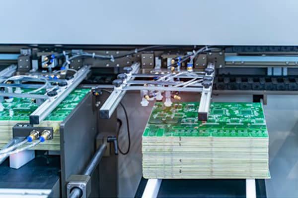
Step 19. Packing
Related PCB Fabrication Services
Related Posts
- Quick Turn PCB Fabrication And Assembly Services In China
- How To Search for a Reliable PCB Manufacturer
- Why Choose Chinese PCB Manufacturer
- Choosing the Right Metal Core PCB Manufacturer is Critical to Your Success
- 6 Tips For Looking For A PCB Prototype Manufacturer
- Low-Cost PCB Prototype Fabrication
- Flying Probe Testing For PCB
- The Application of Thermoelectric Separated Copper Core PCB in the Field of LED Heat Dissipation


