
What is a Surface Mount Device or SMD Component Package?
Home » PCB Assembly » What is a Surface Mount Device or SMD Component Package?
No matter whether you are engaged in the electronic assembly industry or not, I believe you have heard about SMD or SMT or similar terminologies. These are quite common, and you often see and hear these words if you are linked with technology.
Almost all mass-produced electronic products use surface mount technology, but not all components can be surface mount devices (SMDs). In SMT, the dominant type of components is surface mount, but THT is also used.
These professional terms in the industry sometimes make people feel baffled. People usually ask, “what is SMT?” or “what is SMD?” It is necessary to understand these terms. We can only have a deeper understanding of the electronic assembly industry if we understand their definition.
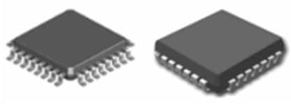
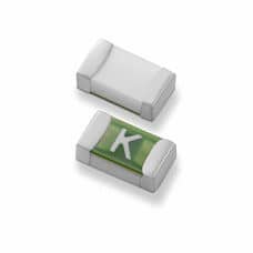
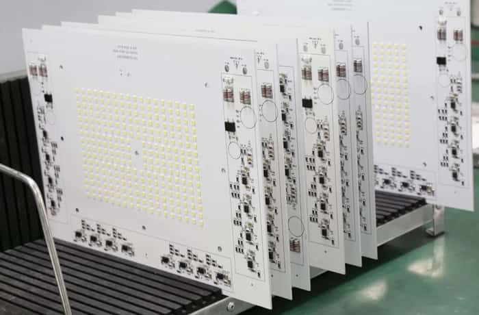
Surface Mount Leaded Components
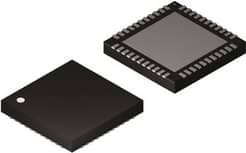
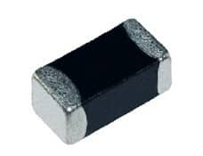
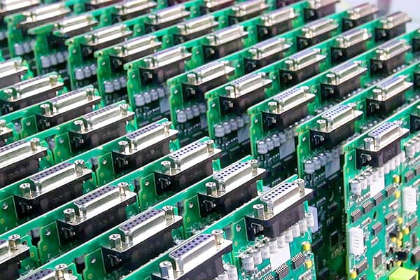
Surface Mount Components without leads
Table of Contents
What is SMD?
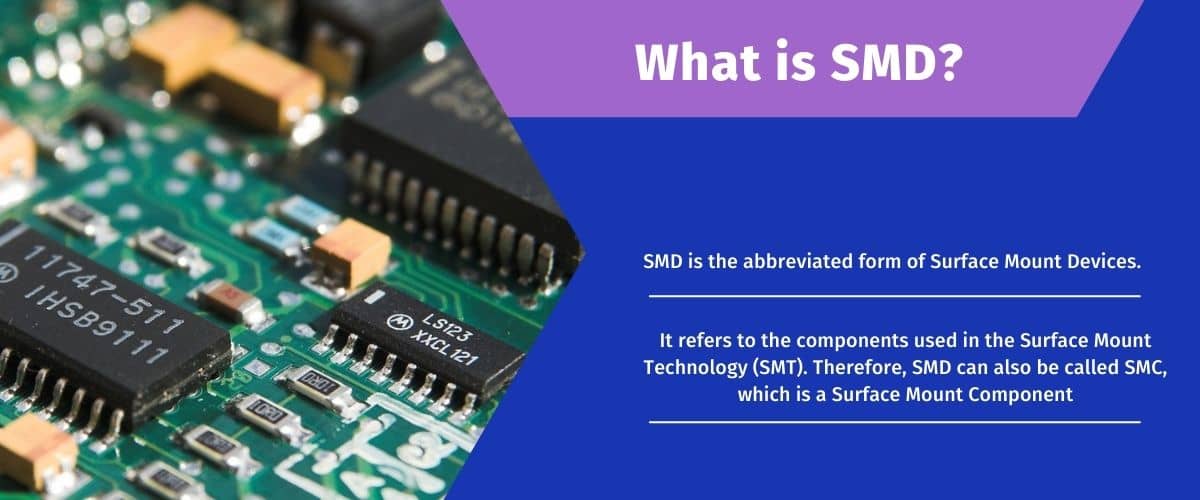
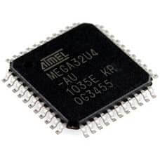
SMD is the abbreviated form of Surface Mount Devices. It refers to the components used in the Surface Mount Technology (SMT). Therefore, SMD can also be called SMC, which is a Surface Mount Component.
SMD has a variety of packaging forms, and most of them have adopted standardized production, which also makes automated PCB assembly a reality and easier.
The following table lists the terms related to surface mount.
| SMp term | Expanded form |
|---|---|
| SMD | Surface-mount devices (active, passive and electromechanical components) |
| SMT | Surface-mount technology (assembling and mounting technology) |
| SMA | Surface-mount assembly (module assembled with SMT) |
| SMC | Surface-mount components (components for SMT) |
| SMP | Surface-mount packages (SMD case forms) |
| SME | Surface-mount equipment (SMT assembling machines) |
The Difference Between SMD and SMT
What is the SMT?
SMT, or Surface Mount Technology, is a new generation of PCB assembly technology. Another PCB assembly technology is Through Hole PCB assembly. So, it is actually a technology, not a component.
SMT is a circuit board assembly technology and is quite popular in the modern electronic assembly industry. The complete SMT process can be divided into five processes, including single-sided assembly and double-sided assembly. Its production equipment includes a solder paste printer, placement machine, reflow oven, optical inspection machine, glue dispenser, etc.
Surface assembly technology has relatively high requirements for the environmental conditions of the production workshop. Generally, dust-free workshops, constant temperature, and low humidity are required, and the staff in the workshops require dust-free clothing, anti-static shoes, gloves, etc.
We have discussed SMT in detail. Let’s understand what SMD is.
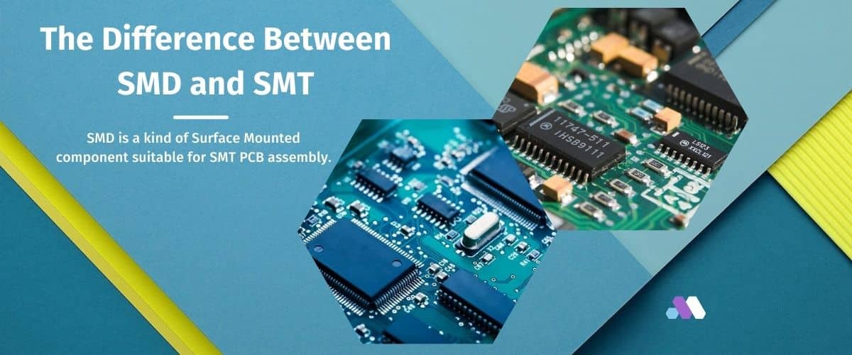
SMD is a kind of Surface Mounted component suitable for SMT PCB assembly. It mainly includes rectangular chip components, cylindrical chip components, composite chip components, and special-shaped chip components, such as CHIP, SOP, SOJ, PLCC, LCCC, QFP, BGA, CSP, FC, MCM, etc.
Advantages of SMT
SMT offers high-density, high-reliability, miniaturization, low-cost, and production automation of electronic product assembly.
- SMT assembly density is high because electronic products can be designed to be smaller and lighter. Therefore, the volume of circuit boards will also become smaller. The volume and weight of SMT components are only about 1/10 of that of traditional plug-in components, which are generally used. After SMT, the volume of electronic products is reduced by 40% to 60%, and the weight is reduced by 60% to 80%.
- It has high reliability and strong anti-vibration ability. The defect rate of solder joints is low.
- It offers excellent high-frequency characteristics and reduces electromagnetic and radio frequency interference.
- It is easy to realize automation and improve production efficiency. It reduces costs by 30%~50% because it saves materials, energy, equipment, manpower, time, etc.
- Using SMT technology, we can design higher-end products, allowing electronic products to be applied to more fields, such as CPUs and smartphones.
- SMT is more suitable for mass production because SMT technology replaces manual plug-in operations with automation. The chip machine is used to place electronic parts, so it is more suitable for mass production of high-quality products, and the quality is more stable.
Characteristics of SMD
The main features of SMD are the shape and structure that are different from the traditional plug-in products.
SMD has a small size, lightweight, short leads or no leads, and high reliability. It offers resistance to shock, vibration, and interference.
SMD is easy to realize semi-automatic and automatic assembly, and most SMD adopts tape and reel, tube, or tray packaging, which is helpful to improve assembly efficiency.
Due to its small size, SMD can achieve high-density assembly, and its solder joint failure rate is less than ten parts per million.
The use of SMD mounting can increase the operating frequency of electronic circuits to 3000MHz (500MHz for through-hole insertion).
It can effectively reduce parasitic parameters, which is conducive to improving the equipment’s high-frequency characteristics and working speed.
The device shape of SMD products is of high dimensional accuracy and consistency.
SMD Technology Adopted By
(1) Laminated Process Technology
In the past, there were three main process methods:
- Mechanical perforation process (dry method)
- Overlap printing process (wet method)
- Internal connection process (wet method)
However, these three process technologies have shortcomings and are difficult to produce smaller and finer chip components effectively.
Now, the mechanical perforation connection process has been greatly improved using laser perforation, close printing, and automatic microporous grouting technology. It has reduced the aperture to 50μm, and the position accuracy is ±20μm. The printing line width and line spacing are 50μm, and its position accuracy is ±10μm. We can produce smaller, more refined chip components and LTCC passive integrated components using this advanced process technology.
(2) Ultra-thin Dielectric Layer and Nano Powder Technology
The current chip multilayer ceramic capacitor (MLCC) capacitance has been increased to 100μf and has been put into practical use. The reason for this is due to the strong support of the ultra-thin dielectric layer and nano-powder technology. The dielectric layer is thin and uniform, indicating the current level of development of ultra-thin dielectric layer technology.
In order to make the ceramic dielectric layer as thin as 1μm, the particle size of the ceramic powder must be nanometers. Metal electrodes must be used instead of Ag/Pd to increase the number of layers to hundreds of layers along with cost considerations. In this way, the development of anti-reduction nano ceramic powder has become a key issue. At present, there have been leaps and bounds in this area at home and abroad.
(3) Thin-Film Technology
In the past few years, thin-film technology was mainly used to manufacture thin-film circuits represented by microwave integration. The cost is quite high, and the production scale is not large.
In recent years, thin-film manufacturing technology has been greatly developed. In addition to traditional physical methods, chemical methods have shown their prowess, bringing thin-film manufacturing technology into a low-cost, large-scale production mode. Chip components manufactured by this process technology have the characteristics of small size, excellent high-frequency characteristics, and easy integration.
(4) Semiconductor Microelectronics Technology
In the last two decades of the 20th century, semiconductor microelectronics technology has made an amazing leap, from micron to sub-micron, and then to deep sub-micron, with high productivity, low cost, and good reliability. The current production level in China has reached 0.18 micrometers. In contrast, the development of passive component manufacturing technology has not been so lucky. In the past few years, passive components have begun to learn from and transplant semiconductor microelectronics technology. Such a wise move has achieved immediate results.
The Development Trend of SMD

(1) High Performance
Driven by the market, performance is improving day by day while the package size is shrinking. Especially in terms of parameter range expansion, the ability to withstand current/power, lead-free production, and reliability has been significantly improved.
(2) Miniature/Thin Profile
People used to think that 1005 (1.0×0.5mm) is the limit of the smallest package size of chip components because such a small package size will bring many difficulties to the mounting process. However, the advancement of surface mount technology makes the package size of the dimensions 0.4×0.2×0.2mm; this is the current mainstream package size. At the same time, the decrease in package size of chip components has not stopped yet and will continue to develop in the direction of miniaturization. We will wait and see how big the package size of SMD devices is.
(3) Arrayization/Componentization
In order to facilitate the application and reduce the occupied PCB area, various chip components have been arrayed.
(4) Integration/LTCC
Passive integration is the current development direction, and low-temperature co-firing (LTCC) is the most suitable passive integration technology. Famous foreign companies, National Semiconductor, Motorola, Murata, etc., have produced a large number of LTCC products, such as radiofrequency modules, Bluetooth modules, etc. These modules are widely used, and the technical difficulty is increasing. LTCC technology has three major technical difficulties: simulation design, special materials, and high-precision process equipment, but domestic and foreign companies have now overcome these difficulties.
(5) High Frequency (Radio Frequency/Microwave)
Modern electronics have a strong trend towards high-frequency development, and most of them are portable. Traditional microwave devices cannot meet the requirements that strongly promote the vigorous development of chip high-frequency (RF/microwave) components.
Specifications of SMD components
With the development of SMT technology, the industry has formed a series of easy-to-operate standard parts, and all parts suppliers manufacture in accordance with this standard.
The standard dimensions of SMD components are as follows:
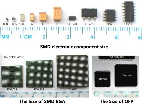
COMMON PASSIVE SMD PACKAGE DETAILS | ||
| SMD PACKAGE TYPE | DIMENSIONS (MM) | DIMENSIONS (INCHES) |
| 2920 | 7.4 x 5.1 | 0.29 x 0.20 |
| 2725 | 6.9 x 6.3 | 0.27 x 0.25 |
| 2512 | 6.3 x 3.2 | 0.25 x 0.125 |
| 2010 | 5.0 x 2.5 | 0.20 x 0.10 |
| 1825 | 4.5 x 6.4 | 0.18 x 0.25 |
| 1812 | 4.6 x 3.0 | 0.18 x 0.125 |
| 1806 | 4.5 x 1.6 | 0.18 x 0.06 |
| 1210 | 3.2 x 2.5 | 0.125 x 0.10 |
| 1206 | 3.0 x 1.5 | 0.12 x 0.06 |
| 1008 | 2.5 x 2.0 | 0.10 x 0.08 |
| 0805 | 2.0 x 1.3 | 0.08 x 0.05 |
| 0603 | 1.5 x 0.8 | 0.06 x 0.03 |
| 0402 | 1.0 x 0.5 | 0.04 x 0.02 |
| 0201 | 0.6 x 0.3 | 0.02 x 0.01 |
| 01005 | 0.4 x 0.2 | 0.016 x 0.008 |
The size of SMD components is composed of 4 digits, the first two digits indicate its length, and the last two digits indicate its width (0.01″ or 10 mils as a unit)
For example, the three most popular sizes are:
0603: means 0.06″x0.03″, or 60×30 mils, or 1.6×0.8mm
0805: means 0.08″x0.05″, or 80×50 mils, or 2.0×1.25mm
1206: means 0.12″x0.06″, or 120×60 mils, or 3.2×1.6mm
Types of SMD
There are many types of SMD, each of which is packaged in a different form, creating a huge library of SMD components.
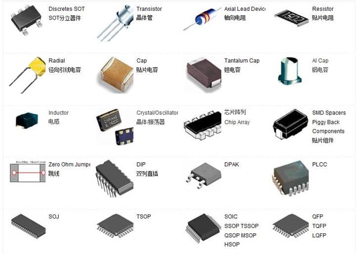
1) The Connecting Member (Interconnect):
It is to provide a mechanical and electrical connection/disconnection by a plug and socket connection composition. The cables, brackets, chassis, or others are for connection, but the actual connection to the plate must be attached to the surface mounted contact.
2) Active and Inactive Electronic Components
- a) Active Electronic Components(Active): Analog or digital circuits can control the voltage and current to produce gain or switching action. It is responsive to signals to which it is applied and can change its basic characteristics.
- b) Passive Electronic Components (Inactive): When an electrical signal is applied, it does not change its own characteristics but provides a simple and repeatable response.
3) Shaped Electronic Components (Odd-form):
These have peculiar geometry dimensions. Therefore, they must be mounted by hand, and the shape of their shell (in contrast to its basic function) is non-standard, such as transformers, hybrid circuit structures, fans, mechanical switch blocks, etc.
According to different classification standards, SMD can also be divided into chip transistors and integrated circuits.
Integrated circuits also include SOP, SOJ, PLCC, LCCC, QFP, BGA, CSP, FC, MCM, etc.
The following briefly introduces the types of SMD components we commonly use.
Note: The letters in brackets represent their identification on the PCB.
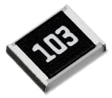
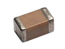
- Chip Resistor (R): A three-digit number on the chip resistor indicates its resistance. Its first and second digits are significant digits, and the third digit represents multiple of 10, such as “103” for “10KΩ”, “472” for “4700Ω”, and the letter “R” for decimal points, for example, R15 = 0.15Ω.
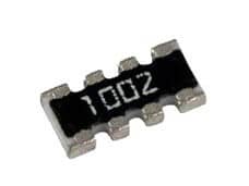
- Network Resistor (RA/RN): It encapsulates several resistors having the same parameters. Network resistance is generally used in digital circuits. The resistance identification method is the same as the chip resistance.
- Capacitor(C): MLCC(Multi-layer Ceramic Capacitors) is the most used type. Based on material, it is divided into COG(NPO), X7R, and Y5V. COG(NPO) is the most stable one. Tantalum capacitors and aluminium capacitors are the other two special capacitors we use. Pay attention while distinguishing the polarities of the two.


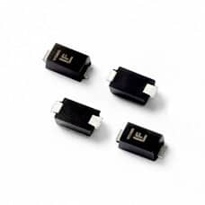
- Diode(D): It is a widely used SMD component. Generally, on the diode body, the color ring indicates the direction of its negative pole.
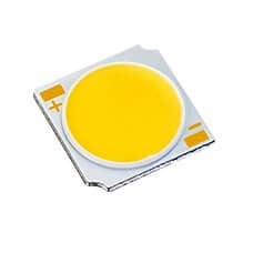
- LED(LED): LED is divided into ordinary LEDs and high-brightness LEDs. The colours are white, red, yellow, blue, etc. The polarity of an LED should be determined according to specific product manufacturing guidelines.
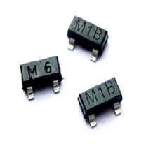
- Triode(Q): Its typical structures are NPN and PNP, including Triode, BJT, FET, MOSFET, etc. The most commonly used SMD packages for components are SOT-23 and SOT-223(larger).
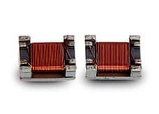
- Inductance(L): The inductance value is generally printed directly on the body.
- Transformer (T): It helps in increasing and decreasing the AC voltage.
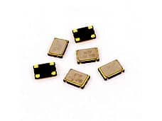
- Crystal oscillator(X): It is mainly used to generate oscillation frequency in various circuits.
- Fuse: It breaks the circuit in case of excess flow of current.
- IC (U): Integrated Circuit (IC) is the most important functional component of electronic products. The package is more complicated and will be described in detail later.
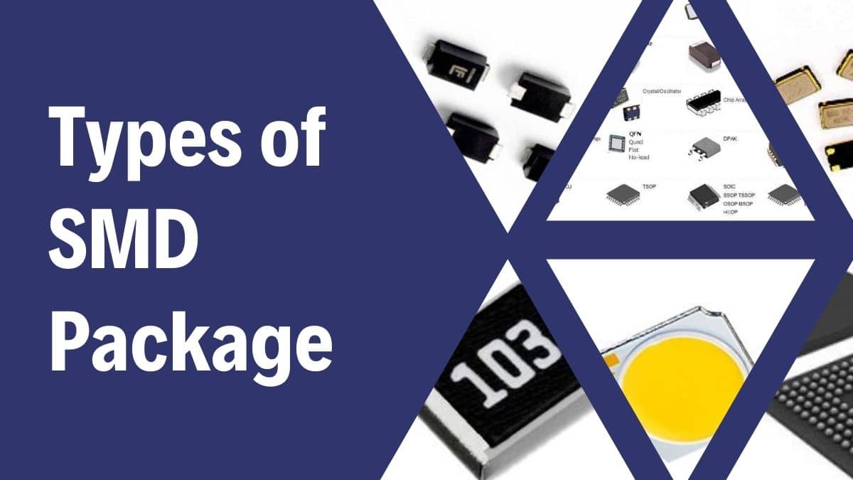
Types of SMD Package
1) BGA (Ball Grid Array)
BGA is one of the surface mount packages, and it has an array of spherical contacts. Spherical bumps are made on the back of the printed circuit board in a display mode to replace the pins. The LSI chip is assembled on the front side of the printed circuit board and then sealed by molding resin or potting. Pins can exceed 200, which is for a multi-pin LSI package.
The package body can also be made smaller than QFP(Quad Flat Package). For example, with a pin center distance of 1.5mm, a 360- pin BGA is only 31 square millimeters. On the other hand, with a pin center distance of 0.5mm, a 304-pin QFP is 40 square millimeters. Moreover, BGA does not have to worry about QFP pin deformation issues.
Motorola Corporation of the United States developed this package. It was first adopted in portable phones and other devices and may be popularized in personal computers in the United States in the future. Initially, the BGA pin (bump) center distance was 1.5mm, and the total number of pins was 225. There are also some LSI manufacturers that are developing 500-pin BGAs.
The problem with BGA is the visual inspection after reflow soldering. It is not yet clear whether an effective visual inspection method is available. Some believe that due to the large center distance of welding, the connection can be regarded as stable and can only be processed through functional inspection.
American Motorola Company calls the package sealed with molded resin as OMPAC, and the package sealed with potting method is called GPAC (see OMPAC and GPAC).
2) BQFP (Bumpered Quad Flat Package)
It is one of the QFP packages with protrusions (buffer pads) that are provided at the four corners of the package body to prevent bending and deformation of the pins during transportation. American semiconductor manufacturers mainly use this package in ASICs such as microprocessors and circuits. The pin center distance is about 0.635mm, and the pin number ranges from 84 to 196. (see QFP).
3) Butt Welding PGA(Butt Joint Pin Grid Array)
It is another name for Surface mount BGA (see surface mount BGA).
4) C-(ceramic)
It indicates the mark of the ceramic package. For example, CDIP stands for ceramic DIP. It is a mark that is often used in practice.
5) Cerdip
Ceramic dual in-line package, sealed with glass, is used for ECL RAM, DSP (digital signal processor), and other circuits. With glass windows, Cerdip is used for ultraviolet erasable EPROM. The pin center distance is 2.54mm, and the number of pins is from 8 to 42. In Japan, this package is expressed as DIP-G (G means glass seal).
6) Cerquad
It is one of the surface mount packages. The ceramic sealed QFP is used for packaging DSP logic under the seal, such as LSI circuits. With windows, Cerquad is used to encapsulate EPROM circuits. The heat dissipation is better than that of plastic QFP, and it can tolerate under natural air-cooling conditions of 1.5 to 2W of power. However, packaging costs three to five times higher than plastic QFP. The center distance between pins has a variety of specifications, such as 1.27mm, 0.8mm, 0.65mm, 0.5mm, 0.4mm, and so on. The number of pins ranges from 32 to 368.
7) CLCC (Ceramic Leaded Chip Carrier)
It is one of the surface mount packages that is a ceramic chip carrier with pins. The pins are drawn from the four sides of the package and are in a T-shape. With windows, it is used to package ultraviolet erasable EPROM and EEPROM microcomputer circuits. This package is also called QFJ, QFJ-G (see QFJ).
8) COB (Chip on Board)
Chip packaging is one of the bare chip mounting technologies. The semiconductor chip is handed over and mounted on the printed circuit board. The electrical connection between the chip and the substrate is made by wire stitching. The electrical connection between the chip and the substrate is covered with resin to ensure reliability. Although COB is the simplest bare chip mounting technology, its packaging density is far inferior to TAB and flip-chip bonding technology.
9) DFP (Dual Flat Package)
Dual Flat Package is another name for SOP (see SOP). This term was common, but it is not used now.
10) DIC (Dual in-line Ceramic Package)
It is another name for ceramic DIP (including glass seal) (see DIP).
11) DIL (Dual in-line)
It is another name for DIP (see DIP). European semiconductor manufacturers often use this name.
12) DIP (dual in-line package)
Dual in-line Package is one of the plug-in packages. The pins are drawn from both sides of the package, and the package materials are plastic and ceramic.
DIP is the most popular plug-in package, and its application range includes standard logic ICs, memory LSIs, and microcomputer circuits. The pin center distance is 2.54mm, and the number of pins is from 6 to 64. The package width is usually 15.2mm. Some packages with a width of 7.52mm and 10.16mm are called skinny DIP and slim DIP (narrow DIP), respectively. But in most cases, no distinction is made, and they are simply collectively referred to as DIP. In addition, ceramic DIP sealed with low-melting glass is also called Cerdip (see Cerdip).
13) DSO (Dual Small Out-line)
Dual Small Out-line package is another name for SOP (see SOP). Some semiconductor manufacturers use this name.
14) DICP (Dual Tape Carrier Package)
Dual Tape Carrier Package is one of TCP (carrying package). The pins are made on the insulating tape and lead out from both sides of the package. Due to the use of TAB (Automatic On-Load Soldering) technology, the package outline is very thin. It is often used in LCD driver LSI, but most of them are customized products. In addition, the 0.5mm thick memory LSI book package is in the development stage. In Japan, in accordance with the EIAJ (Electronic Industries Association of Japan) standards, DICP is named DTP.
15) DTP (Dual Tape Carrier Package)
It is the same as above DICP. The Electronic Industries Association of Japan names it DTP.
16) FP (Flat Package)
Flat Package is one of the surface mount packages. It is another name for QFP or SOP (see QFP and SOP). Some semiconductor manufacturers use this name.
17) Chip
Flip-chip welding is one of the bare chip packaging technologies to make metal bumps in the electrode area of the LSI chip and then connect the metal bumps with the electrode area on the printed circuit board.
The footprint of the package is basically the same as the chip size. It is the smallest and thinnest of all packaging technologies. However, if the thermal expansion coefficient of the substrate is different from that of the LSI chip, a reaction will occur at the joint, which will affect the reliability of the connection. Therefore, it is necessary to use resin to reinforce the LSI chip and use a substrate material with substantially the same thermal expansion coefficient.
18) FQFP (Fine Pitch Quad Flat Package)
FQFP usually refers to the QFP with a lead center distance less than 0.65mm (see QFP). Some conductor manufacturers use this name.
19) CPAC (Globe Top Pad Array Carrier)
American Motorola Company’s nickname for BGA (see BGA).
20) CQFP (Quad Flat Package with Guard Ring)
It is a four-side pin flat package with a guard ring. It is one of the plastic QFPs in which the pins are masked with a resin protection ring to prevent bending and deformation. Before assembling the LSI on the printed circuit board, cut the lead from the guard ring and make it into a seagull wing shape (L shape). This kind of package has been mass-produced by Motorola Company in the United States. The pin center distance is 0.5mm, and the number of pins is about 208 at most.
21) H- (With Heat Sink)
It means a radiator. For example, HSOP means SOP with a heat sink.
22) Pin Grid Array (Surface Mount Type)
Usually, PGA is a plug-in package with a pin length of about 3.4mm. The surface mount PGA has display-like pins on the bottom surface of the package, and its length ranges from 1.5mm to 2.0mm. Mounting uses the method of butt welding with the printed circuit board, so it is also called butt welding PGA. Because the pin center distance is only 1.27mm, which is half smaller than the plug-in type PGA, the package body cannot be made so large. The number of pins is more than that of the plug-in type (250~528), which is a package for large-scale logic LSIs. The encapsulated substrates include multilayer ceramic substrates and glass epoxy resin printing bases. The packaging of multilayer ceramic substrates has been put into practical use.
23) JLCC (J-leaded chip carrier) J-leaded Chip Carrier
It is another name for CLCC with window and ceramic QFJ with window (see CLCC and QFJ). Some semiconductor manufacturers adopted the name.
24) LCC (Leadless Chip Carrier)
Leadless Chip Carrier refers to a surface-mount package in which the four sides of the ceramic substrate are only in contact with electrodes without leads. It is an IC package for high-speed and high-frequency, also called ceramic QFN or QFN-C (see QFN).
25) LGA (Land Grid Array)
Contact Display Package is a package with array state electrode contacts that are made on the bottom surface. Just plug in the socket when assembling. There are now practical ceramic LGAs with 227 contacts (1.27mm center distance) and 447 contacts (2.54mm center distance), which are used in high-speed logic LSI circuits.
Compared with QFP, LGA can accommodate more input and output pins in a smaller package. In addition, since the impedance of the lead is small, it is very suitable for high-speed LSI. However, due to the complicated production and high cost of sockets, they are basically not used much now. It is expected that its demand will increase in the future.
26) LOC (Lead on Chip)
Chip Lead Package is one of the LSI packaging technologies. It has a structure in which the front end of the lead frame is above the chip, bump solder joints are made near the center of the chip, and wire stitching is used for electrical connection. Compared with the original structure in which the lead frame is arranged near the side of the chip, the chip is contained in the same size package and has a width of about 1 mm.
27) LQFP (Low Profile Quad Flat Package)
Thin QFP refers to the QFP with a package body thickness of 1.4mm. It is the name used by the Japanese Electronic Machinery Industry according to the new form factor formulated QFP.
28) One of L-QUAD
Aluminum nitride is used for packaging substrates that have a thermal conductivity 7-8 times higher than aluminum oxide and have better heat dissipation. The frame of the package is aluminum oxide, and the chip is sealed by potting, thereby suppressing the cost. It is a package developed for logic LSI, which can tolerate W3 power under natural air-cooling conditions. 208-pin (0.5mm center distance) and 160-pin (0.65mm center distance) LSI logic packages have been developed, and mass production began in October 1993.
29) MCM (multi module)
It is a package in which multiple semiconductor bare chips are assembled on a wiring substrate. According to the substrate material, it can be divided into three categories: MCM-L, MCM-C, and MCM-D.
MCM-L is a component using a common glass epoxy multilayer printed circuit board. The wiring density is not very high, and the cost is low. MCM-C uses thick film technology to form multilayer wiring and uses ceramic (alumina or glass-ceramic) as a substrate component, which is similar to a thick film hybrid IC using a multilayer ceramic substrate. There is no obvious difference between the two. The wiring density is higher than MCM-L. MCM-D uses thin-film technology to form multilayer wiring, with ceramic (aluminum oxide or aluminum nitride) of Si or Al as the substrate component. The wiring scheme is the highest among the three components, but the cost is also high.
30) MFP ( Mini Flat Package)
It is another name for plastic SOP or SSOP (see SOP and SSOP). It is the name adopted by some semiconductor manufacturers.
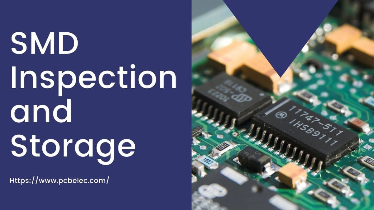
SMD Inspection and Storage
To ensure that all moisture-sensitive devices are effectively controlled during storage and use, avoid the following two points:
- a) The parts are affected by dampness, which affects the welding quality.
- b) Moist parts will cause cracks in the plastic body and pins when heated at instantaneous high temperatures. A slight crack will cause leakage of the shell, and the chip will slowly fail due to moisture, which will affect the life of the product, and severe cracks will directly destroy the component.
- All plastic-encapsulated SMD parts are sealed in moisture-proof packaging before leaving the factory, and no one can open it at will. The warehouse clerk receives the material, and IQC confirms the package by inspecting the SMD model and quantity of the parts. When the package is opened, the number of openings should be minimized. After inspection, the SMD parts should be put back into the original package and then sealed after vacuuming with a vacuum machine.
- All SMD parts that have been opened will be prioritized to go online as much as possible.
- There are special storage environment requirements for moisture-sensitive parts. The room temperature should be less than 30℃, and the relative humidity should be less than 75%.
PCB, QFP, and BGA components should be used up within 12 hours after the package is opened; SOIC, SOJ, and PLCC components must be used within 48 hours after the package is opened.
- If the SMD parts are not used after opening, repack them into the bag, put a desiccant inside, and seal the mouth after vacuuming with a vacuum machine.
- When using SMD parts, first check the humidity value of the humidity indicator card. If the humidity value is 30% or above, it needs to be baked. The company uses SMD parts to equip the humidity indicator card with six circles, and the humidity is respectively 10%, 20%, 30%, 40%, 50%, and 60%.
How to read: If the 20% circle turns pink, the 40% circle still displays blue, and the next circle is lavender (between blue and pink), then the humidity value is 30%.
- When opening the package, if it is found that the humidity of the indicator card is 30% more, it needs to be dried at a high temperature. The oven temperature should be 125℃±5℃, and the drying time is usually 5~48 hours. The specific temperature and time vary from different manufacturers, so it is better to refer to the manufacturer’s drying instructions.
- QFP’s packaging plastic tray has two types: non-high temperature resistant and high temperature resistant. The high-temperature resistant ones are Tmax=135, 150, or 180℃, which can be directly put into baking. The non-high temperature-resistant trays cannot be directly put into the oven.
SMD Inspection
The main inspection items of components include solderability, pin coplanarity, and usability, and it is done by the inspection department. To test the solderability of components, hold the component body with stainless steel tweezers, immerse it in a tin pot at 235±5℃ or 230±5℃, and take it out after 2±0.2s or 3±0.5s. Check the soldering end of the solder under a 20 times microscope. It is required that more than 90% of the soldering end of the component is soldered.
As an SMT chip processing workshop, the following visual inspections can be done:
- Visually or with a magnifying glass, check whether the solder ends or pin surfaces of the components are oxidized or have no contaminants.
- The nominal value, specification, model, precision, external dimension, and other things of components should be consistent with the production and process requirements.
- The pins of SOT and SOIC cannot be deformed. For multi-lead QFP devices with a lead pitch of less than 0.65mm, the pin coplanarity should be less than 0.1mm (which can be optically detected by the placement machine).
- For products that require cleaning, the mark of the components will not fall off after cleaning and will not affect the performance and reliability of the components (visual inspection after cleaning is needed).
How Does FPC Adopt SMT Assembly Technology?
The process requirements for mounting SMD on a flexible printed circuit board (FPC):
When the miniaturization of electronic products develops, a considerable part of consumer products is surface mount technology. Due to the compact designs and minimal assembly space, the SMD is mounted on the FPC. The surface mounting of SMD on FPC has become one of the development trends of technology. The process requirements and attention points of surface mounting have the following points.
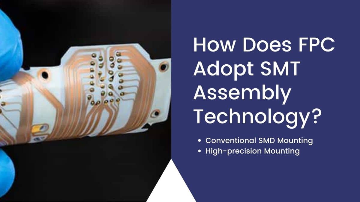
Conventional SMD Mounting
features: mounting accuracy is not high, The number of components is small, and the types of components are mainly resistors and capacitors, or there are individual special-shaped components.
Key Process:
- Solder Paste Printing: FPC is positioned on the special pallet for printing according to its appearance. Generally, it is printed by a small semi-automatic printing machine. Manual printing is used, but the quality of manual printing is worse than that of semi-automatic printing.
- Mounting: Generally, manual mounting can be used, and individual components with higher position accuracy can also be mounted by a manual placement machine.
- Welding: The reflow welding process is commonly used, but spot welding can also be used under special circumstances.
High-precision Mounting
features: The FPC must be marked for substrate positioning, and it must be flat. It is because it is difficult to fix FPC, and consistency is difficult to ensure during mass production. It also requires high-end equipment. In addition, it is more difficult to control the printing of solder paste and the mounting process.
Key Process:
- FPC Fixing: FPC is fixed on the pallet from the printing patch to the reflow soldering. The pallet used requires a small thermal expansion coefficient. There are two fixing methods, and they are used according to the conditions. When the placement accuracy of QFP lead spacing is above 0.65mm, use method A. If it is below 0.65mm, use method B.
Method A: The pallet is placed on the positioning template, and the cradle FPC is fixed on with a thin high-temperature tape. Then let the pallet separate from the positioning template for printing. The high-temperature resistant tape should have a moderate viscosity, it must be easy to peel off after reflow soldering, and there should not be residual glue on FPC.
Method B: The pallet is customized, and in this process, it is required that the deformation must be minimal after multiple thermal shocks. The pallet is equipped with a T-shaped positioning pin, and the height of the pin is slightly higher than the FPC.
- Solder Paste Printing: Because the pallet is loaded with FPC, the FPC has positioning resistance. The high-temperature tape makes the height inconsistent with the plane of the pallet, so an elastic scraper must be used when printing. The composition of the solder paste has a greater impact on the printing effect, so the appropriate solder paste must be selected. In addition, the printing template of method B needs to be specially processed.
- Mounting equipment: First, the solder paste printer should have an optical positioning system; otherwise, the welding quality will have a greater impact. Secondly, the Flexible PCB is fixed on the pallet, but there will always be some tiny gaps between the flexible PCB and the pallet, the most significant difference from the rigid PCB. The setting of equipment parameters will have a greater impact on the printing effect, placement accuracy, and welding effect. Thus, the FPC placement requires strict process control.
Lastly, in order to ensure the quality of assembly, it is best to dry the FPC before mounting.
Related PCB Assembly Services
Related Posts
- PCB Assembly Capability
- The Main PCB Assembly process Steps
- Components Purchasing Services
- What is the Bill of Materials(BOM), and how to create one?
- The Production Process and Specifications of PCB SMT stencil
- Solder Paste and Solder Paste Printing in SMT PCB Assembly
- What is the difference between SMT and SMD?
- What is the difference between wave soldering and reflow soldering?
- How to Use PCB Stencil-Step by Step Guideline
The following is a detailed document about surface mount naming and packaging for free download.
This article is very long; we have converted this page into a PDF document. You can download it and read it later.