
What Is Flex PCB Prototyping?
Rapid Flex PCB Prototype Fabrication
Home » Prototype PCB » What Is Flex PCB Prototyping?
Flex Circuit Prototyping Applications
Flex PCB prototyping and its application are common in modern-day electronics, with the earliest description filed in a patent in the early 1900s. Flex PCB Prototyping used in flex PCB manufacturing is used in keyboards, mobile phones, smartwatches, printers, and other industrial applications in modern electronics. With the recent trend of electronics getting smaller, flex PCB prototyping and its design have increased.
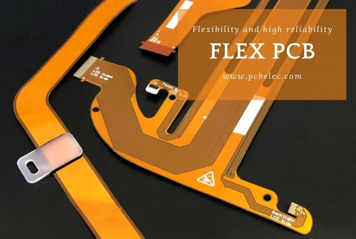
What Is Flex PCB?
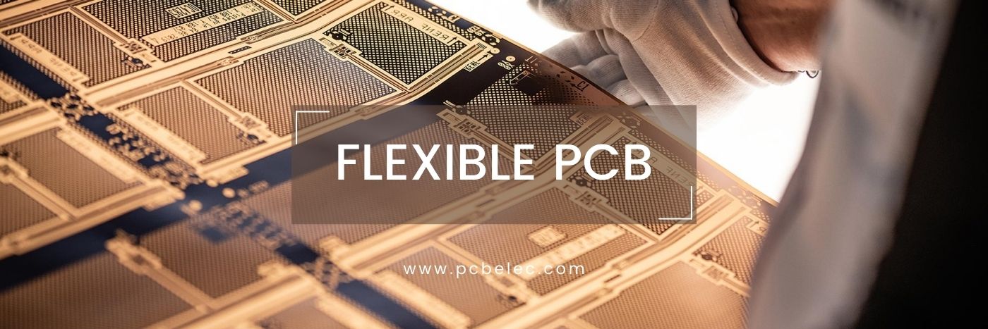
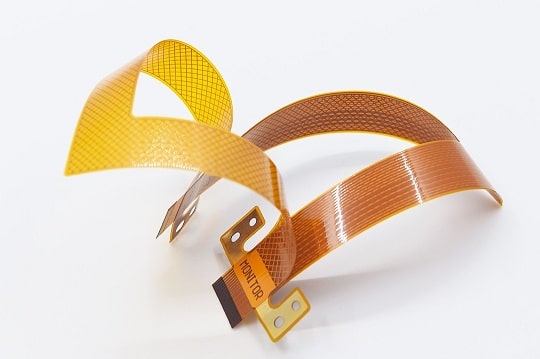
Flex PCBs are an essential component of our common electronics like mobile electronic devices, desktop printers, and hard disks. Comprising of a strong substrate material with or without overlay, Flex PCBs consist of various complex components. Flexible PCB is a printed circuit board that is made of PET (Polyester) or polyimide, with excellent flexibility and high reliability.
Due to the flexibility and advancement in flexible PCB technology, manufacturers of electronics are more inclined to develop the prototype of these devices before manufacturing. This is due to the fact that the flex PCB prototypes create an avenue for the manufacturers to identify errors and make necessary changes before the product is introduced in the market.
What Is Flex PCB Prototyping?
Flex PCB prototyping describes the process of developing quick and functional replicas or models of products manufactured through naturally flexible substrate materials. Flex PCB Prototyping is an important technology used to manufacture advanced and modern electronic products. Flex PCB Prototyping offers the following benefits to flex PCBs in their various applications:
- Lightweight. The flex circuit’s polyimide material is lighter than FR4.
- Flexible. This is obvious, but you have more freedom to decrease the overall mechanical footprint with the ability to make bends.
- Thin. A typical 2-layer flex can range in thickness between 4.4 and 10 mils.
- High Temperature. Polyimide flex materials are suited for very high temperatures compared to FR4. They are also resistant to oils, gases, and acids.
Where Is Flex PCB Prototyping Used?
Flex PCB prototyping has various applications including these industries:
- Medical
- Aerospace
- Consumer Electronics
- Communications
- Industrial
- Automotive
- Transportation
- Military
Related Reading: Development and Applications of FPC Flexible PCB
What Are The Benefits Of Using Flex Printed Circuit Prototyping?
- They are lightweight and thin and therefore lend themselves to miniaturization.
- As their name suggests, they offer flexibility and hence more freedom to decrease the mechanical footprint.
- Flex PCB prototypes are resistant to high temperatures, oils, gases, and acids.
- Flex PCB prototyping is highly durable. The reduced number of interconnects allows them to handle changing forces and improve their resistance to shock.
- They have high signal integrity.
- They can support high circuit densities.
- They lend themselves to reduced wiring errors.
- On account of fewer assembly steps involved, they tend to be relatively low-cost
- They offer improved heat dissipation.
What Is The Flex PCB Classification?
Single layer flex PCBs are cheaper relative to other classes of PCBs but with a low electrical performance PCB. It is the perfect choice for engineers when wiring is positioned on one side of the board. Through chemical etching, the conductive pattern on the substrate is a rolled copper foil. The Insulating base material may be PET, polyimide, PVC, and aramid fibers.
Double-sided Flex PCBs have chemically-etched conductive patterns on both sides of the insulating base. Metallic holes are used as the electronic connection between the insulating layers to suit the design function and flexibility. The covering film can protect the connections and show the components locations.
Multilayer flex PCBs are laminated with over three layers of single or double-sided flex circuits. This creates a conductive path between various layers of the laminated circuits with metallic holes drilled. Multilayer circuits have better reliability, improved thermal conductivity, and enhanced convenience in assembly performance. The layers, flexibility, and assembly dimension should be taken into account when designing.
Rigid-Flex circuit PCBs consist of a combination of flexible and rigid circuit boards which are connected permanently to each other. The right application of Rigid-Flex PCBs provides the best solutions for difficult and limited space conditions. Rigid-flex PCB technology provides the possibility of a secure connection of device components with the assurance of polarity and contact stability, and a reduction in plug and connector components. Another advantage of Rigid-Flex PCBs is mechanical and dynamic stability, three-dimensional design, easy installation, space savings, and the maintenance of uniform electrical characteristics. The application Rigid-Flex PCBs can minimize the total cost of the finished product. A standard manufacturing process that adopts IPC guidelines assured of a reliable and economical product, which is UL Certified with no additional cost. Depending on the type of application, a complete Rigid-Flex printed circuit board might be manufactured either asymmetrically or symmetrically with outward or inward flexible layers respectively.
What Is The Flex PCB Price?
In the PCB industry and market segment, determining the price of flex PCBs can be tricky. With manufacturers segmenting the PCB market by volume, market desirability, time of delivery, and strategies for targeted customer penetration; it’s easy to understand the reason behind the significant variation of flex PCBs among various suppliers. This difference can be complicated further by how engaged a factory is at any given time. With these constantly changing variables, it is quite difficult to make generalizations about the pricing and costs of flex PCBs.
While several factors have an impact on the fabricating cost of a flex circuit, these three cost factors are common:
- Physical Size: This is important, but not as easy as the computation of the area of a square inch. In flex PCB industry and market segment, prices are mostly quoted in per square inch (es).
- Circuit Construction: A major factor that also affects the flex PCB price is the quantity of conducting layers. Two layers (Double-sides) circuits will always have a price that is at least 1.5 times a circuit of single layer and equivalent size. The costs of materials are one of the reasons, however the additional capital intensive equipment and the steps involved in processing the flex PCBs are a huge factor.
- Volume: Even though there are some shops that specializes in quick turnover and delivery and low volume flex PCBs, most of the fabricators try to compensate for overhead and engineering costs using low volume designs. The support of the suppliers for low volume designs is necessary especially if more volumes are to be taken into consideration. Much charge for quantity of flex PCBs with low volume are quite common. A cost-effective method of tooling called “Soft tooling” is required to cover some costs for each circuit as the circuits are customized and requires unique artworks, electrical test designs, drill files, excusing files, and inspection files. A one-off charge should be expected also.
How To Make Flex PCB Prototyping?
Flex PCB Prototyping is made through the following process:
- Flex PCB Stackup: This is a significant part of a flex PCB design data set. It comprises a flex PCB description explaining and completing the particular material requirements and its construction. The flex printed product supplier needs circuit board stack-up to ensure the finished product is manufactured in accordance with customer specifications and meets all electrical and mechanical bending design requirements.
The flex PCB stack-up comprises the appropriate amount of data and information. It describes the type of materials to be utilized, where they are located, their respective layer of thicknesses, their part numbers, and the thickness of all the design areas. Most flex circuitry designs have multiple constructions that create different thickness requirements. Some areas may have thicknesses that may significantly affect the circuitry’s performance, either in meeting a particular bend requirement, connector specification (for example, ZIF connectors), or impedance value.
These particular requirements include:
- Non-Adhesive flex core(s)
- Distinctive overlays are applied only to exposed flexible areas and shouldn’t be applied to rigid regions.
- Non-flowing prepreg required for the lamination of the rigid layer and high Glass transition temperature FR4 rigid core
The flex PCB includes flex cores, coverlays/solder masks, stiffeners, and other materials listed below.
Flex Cores:
- Types: (Non-adhesive or Adhesive)
- The thickness required: Copper weights
- Type of Copper: (RA or ED)
- Lamination: Thickness of Adhesive
Soldermask/Coverlays:
- Adhesive Thickness
- Thickness
- Color
- Adhesive Type (Acrylic, Epoxy, and others.)
- Type of Material (Aluminum, FR4, Polyimide, Stainless, and others)
- Attachment Adhesive (Thermally bonded or PSA)
- Thickness
Additional Materials Required:
- EMI Shielding Film
- Epoxy Strain Relief
- Pressure Sensitive Adhesive (PSA)
Related Reading
- Knowledge of Plating on Flexible Circuit Board Surface
- Knowledge of Flexible Printed Circuit Board Processing Technology
- The terms you have to know related to the manufacture of Flexible PCB
- Complete Introduction To Flexible PCB Assembly Process
- How to Solder On Flex PCB?
- The Manufacturing Process Of Double-sided Flexible PCB Coverlay
Flex PCB Thickness
Flex PCBs design usually have a thickness tolerance that is between ±30um and 50um when finished. Depending on the layer counts, the thickness tolerance might be larger. The thickness may also vary as a result of where the parts are measured or the reduced thickness of the adhesives after lamination because of consumption of the part of the materials when spaces between the traces are filled.
Related Reading
Flex PCB Manufacturing Process
Flex PCB manufacturing process involves the following:
Material Preparation (Pre-Clean) Production panels chemically cleaned, before application of circuit forming photoresist film, to ensure proper film adhesion.
Conveyorized process utilizing thin core handling equipped systems to prevent damage to ultra-thin material cores.
Circuit Pattern Exposure Photo resist coated panels, overlayed with circuit artwork patterns, exposed with collimated UV light to transfer circuit image(s) to production panels. Both sides are exposed simultaneously if required.
Etch Process Circuit patterns chemically etched using specialized thin core handling equipped conveyorized systems. Both sides of panels are etched simultaneously if required.
Drilling Process High speed, high precision, small hole capable, drilling systems create required circuit hole patterns in production panels. Laser-based systems are available for ultra-small hole requirements.
Copper Plating Process Fully automated electrolytic copper plating systems deposit required additional copper within plated through holes to form a layer to layer electrical interconnects.
Coverlay Application Polyimide Coverlays aligned and tacked into place on production panels before the Coverlay lamination process.
Stiffener Application Localized additional stiffeners (if required by specific design) aligned and applied before additional lamination process under heat, pressure, and vacuum.
Electrical Test100% net list driven electrical test per IPC –ET-652. Simultaneous testing of all circuits for continuity and isolation. Both grid and flying probe test systems were utilized.
Final Fabrication Individual parts die cut from production panel using high precision male / female punch and die sets. Other methods include laser cutting, mechanical routing, steel rule dies, and chemically milled dies depending upon specific design requirements.
How To Choose The Flex PCB Prototyping Manufacturer?
The following is required in choosing the flex PCB Prototyping manufacturer:
- Superior Facility: The manufacturer’s advanced manufacturing equipment and professional technicality should allow the manufacturer to produce flex PCB prototypes of high quality that stand out in the market. The manufacturer’s engineers should be experienced and follow the best practices required by the PCB industry.
- Strict Adherence to Industry Standards: A manufacturer cannot cut corners for flex PCBs prototyping. The manufacturer must ensure strict compliance with best practices and industry standards. Also, the manufacturer must have robust test procedures.
- Fast Turn-Around or Processing Time: The manufacturer’s quick turnaround time ensures that the frequency of you visiting the market is reduced significantly and your advantage competitively is heightened.
- Easy To Expand: The main advantage of associating with a manufacturer is to provide a quality flex PCB prototype and guarantee scalability.
- Strict and Rigorous Tests on PCB Components: With advanced projects, a manufacturer must ensure stringent testing exists for each component to identify errors and flaws where there are any. This leads to needed replacements and guarantees flex PCB prototype viability.
Flex PCB Prototyping FAQs
Most frequent questions and answers
The reason why flex PCB prototyping is so important is to conduct small-scale trial production to verify the rationality and manufacturability of the design before mass production. Flexible PCB prototyping can quickly eliminate design errors, improve design solutions, and save costs due to errors.
Yes, our experienced PCB engineers and technicians will provide customers with a complimentary design for manufacturability check service to ensure that your flexible PCB prototypes are as perfect as possible.
Yes, we have advanced flexible PCB manufacturing equipment and rich experience in flexible PCB manufacturing. We will provide you with highly reliable and affordable double-sided flexible PCB and multi-layer flexible PCB manufacturing services.
Yes, we offer a rapid flex PCB prototype fabrication service. Our fast turnaround service supports 24 hours or same-day lead times.
Yes, our original intention is to provide customers with high-quality, high-reliability, and cost-effective flexible PCB prototyping services.
Yes, we can provide a fast flex PCB prototype assembly service. We have multiple PCB assembly lines, and our assembly capabilities include surface mount technology, through-hole assembly technology, and more.
No, we have no MOQ requirement. We offer flexible PCB prototypes with no MOQ and small to medium volume manufacturing and assembly services.
You can submit your inquiry information through our online form, or you can send Gerber and BOM to sales@pcbjhy.com for a quote.
Related Reading
- Why is Flexible PCB so Expensive?
- What Is Flexible PCB Coverlay (FPC Cover Layer)?
- The Manufacturing Process Of Double-sided Flexible PCB Coverlay
- What Are The Advantages And Applications Of Rigid-Flex PCBs?
- Rigid PCB vs Flex PCB: What Is The Difference?
- What Are Flexible PCB Stiffeners?
- 16 Factors Affecting The Cost And Price of Flexible PCB
- How to Make Low Cost PCB Prototypes