
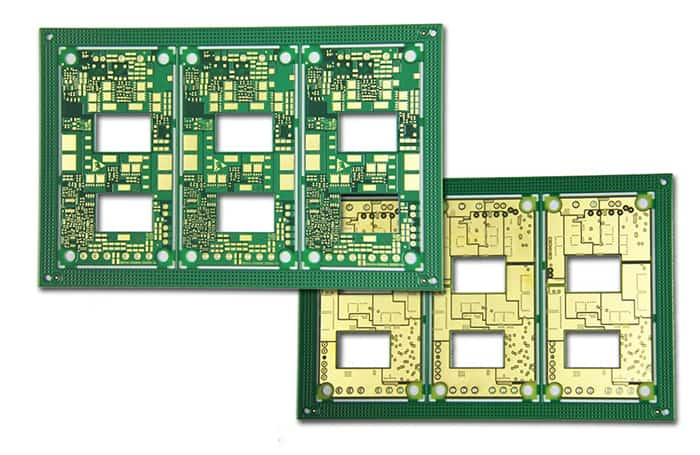
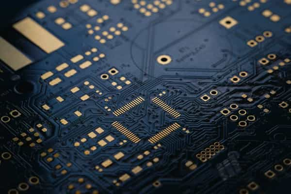
Heavy Copper PCB Fabrication Service
Heavy Copper PCB, Thick Copper PCB or Extreme Copper PCBs have special requirements. JHYPCB is a professional PCB manufacturer in China, can help you verify your design and provide Prototype through Assembly services.
Home » PCB Manufacturing » Heavy Copper PCB
Thick Copper PCB-A Special PCB Board
PCBs are an essential part of almost any electrical product, equipment, or appliance. It is a must because it creates a compact and reliable path for the flow of current. There are different types of PCBs available, and all of them are used for various purposes. One type of PCB cannot fulfill all requirements and bear environmental constraints.
Some products require a heavy current flow in the circuit. This is a particular case where standard PCBs cannot be used. To pass-heavy current from the circuit, the copper/conductive layer must be thicker than usual, and this is where the heavy copper PCB plays its role.
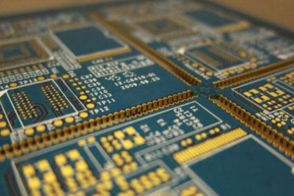
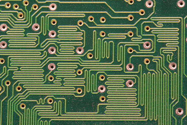
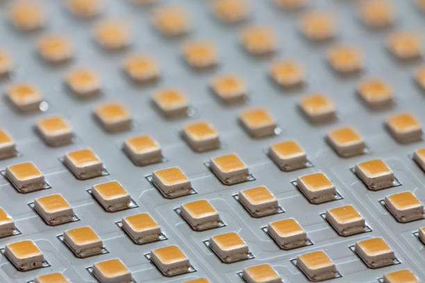
Heavy Copper Printed Circuit Boards
What is Heavy Copper PCB Board ?
A heavy copper PCB is what its name suggests because it contains a heavy amount of copper. The copper/conductive layer on a heavy copper PCB is capable of conducting a high magnitude current.
According to the industry thumb rule, any PCB with a copper thickness from 4oz/ft2 to 20oz/ft2 is called Heavy Copper PCB. Due to the high thickness of copper, the conducting capability of the traces increase, which is why heavy copper PCBs are used for applications where excessive current flows from the circuit.
Why Heavy Copper PCBs?
Heavy copper PCBs are widely used in the industry, but do we really need them in our circuits?
In simple words, heavy copper PCBs are essential for applications where a high current flow is required. Without heavy copper traces, a standard PCB can’t bear a high current flow.
The science behind it is pretty simple. Whenever current flows through a circuit, the components use electrical energy, but it is not 100% efficient. There are heat losses that are commonly known as I2R losses. Common PCBs cannot take away the heat from the board as heavy copper PCBs do, so the components and the board will become overheated, and they stop working due to the failure of components. Thus, a standard PCB cannot deal with heavy current.
The Power Dissipated can be given as I2R. According to the relation, the magnitude of current significantly affects the generated heat. Heat increases drastically, and it is visible from the square power of the current. We cannot reduce current because of the load, but we still have another factor, which is resistance. Heavy copper traces have lower resistance compared to thin traces. The most important thing about heavy copper PCBs is that they can easily flow heavy currents and help in taking the heat away from the board. There can be heat sinks, and the traces transfer heat to them.
Heavy copper PCBs are the perfect solution to regulate heat losses and provide reliable performance in applications where excessive current flows.
JHYPCB has reliable processes to produce copper layer thicknesses up to 400µm(11.4oz) (also for multilayers).
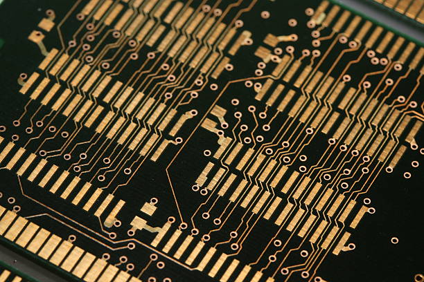
Types of Heavy Copper PCB
Thick copper PCB is divided into single-layer thick copper board, double-sided thick copper board and multilayer thick copper plate.
PCB Copper Thickness Guidelines
Conversion of Copper Thickness Units
The copper thickness of printed circuit boards is calculated in OZ. 1oz means the average weight of copper foil is 28.35g per square foot. Oz is the abbreviation of an ounce. It is a unit of measurement in the English system.
The thickness of copper is the average thickness of copper foil expressed by the weight per unit area. It is expressed by the formula, that is, 1OZ=28.35g/FT2.
Weight unit:
- 1oz=28.35g
- 1oz=16 dram
- 16oz=1 pound
Conversion method:
The weight of copper foil divided by the density and surface area of copper is the thickness of copper foil.
1 square foot = 929.0304 square centimeters, copper density = 8.9kg/dm^3
Let the Copper thickness be X and solve the equation:
X*929.0304c㎡ *8.9 g/cm³=1oz=28.35 g
X=0.0034287cm=34.287um
So, 1oz=34.287um
The thickness of 1OZ copper foil is about 35um or 1.35mil.
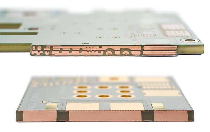
Performance of Thick Copper PCB
Thick copper PCB has the best elongation performance and is not limited by the processing temperature. It can be used in hot melt welding methods such as oxygen blowing at a high melting point and not brittle at low temperatures. Even in extremely corrosive atmospheric environments, copper PCB forms a strong, non-toxic passivation protective layer.
Benefits of Heavy Copper PCBs
Heavy copper PCBs can deal with high-temperature stress as they have excellent thermal conductivity. Due to the increase in copper thickness, copper can carry more current. With the increase in current, the heat dissipation also increases; however, the copper traces conduct heat away with the help of heat sinks present on the board. Moreover, the traces can also dissipate heat in the surrounding. Thus, the PCB has the capability to handle high thermal stress.
The thermal stress that a heavy copper PCB can bear depends on its substrate and the cooling of the PCB. The maximum amount of current is calculated to ensure optimal performance.
The primary advantage of heavy copper PCBs is that they can be used in high-power applications. The current flow is excessive in such applications, so normal PCBs cannot provide optimal performance and might suffer wear and tear because of heat dissipation. Heavy copper PCBs have thick copper traces that can conduct more current; thus, it is suitable for high-power applications.
With the excess use of copper, the circuit develops more mechanical strength. The layers on the circuit are also reduced; consequently, the structure becomes stronger. A heavy copper PCB can bear more mechanical stress than a simple PCB.
Due to excellent heat dissipation, the life of the components and the board is increased. At the maximum current carrying capacity, the heat dissipation is equal to the rate of cooling. Therefore, there is no overheating of the components and high-temperature stress on the board. Consequently, the components provide the optimal result for a long span.
The circuit becomes more compact. A heavy copper PCB can have heavy copper traces for high power applications and low copper traces for controlling. All this can be achieved in a single PCB, which makes the PCB more compact. You can accommodate different copper thicknesses in one PCB; thus, there is no need to create multiple boards for the project. The size of the product is greatly reduced as there are no extra PCBs and connectors.
Why Use Heavy Copper PCBs?
What thick copper can do? (Over 500um / 14.3oz)
Specific printed circuit boards are designed to produce more amperage (or the strength of the electrical current) through the trace. But the higher the power requirement, the thicker the copper you need to transmit the signal through the board. That is why heavy copper PCBs are used in higher amperage designs.
Applications of Thick Copper PCB
Due to the high-current capacity, high power transmissions, and heat-dissipating characteristics of heavy copper PCBs, they are widely used in various industries. They are preferred where reliability and performance are required under high current and temperature stress. The applications that carry out higher load percentages have an excessive current flow, which is why normal PCBs cannot work in these cases. The only solution to the problem is heavy copper PCBs.
You will see heavy copper PCBs in the following areas/applications/industries,
- Military
- Industrial equipment
- Power distribution
- DC-DC converters
- Inverters
- Power supplies
- Protection relays
- Automobiles
- HVAC systems
- Motor controls
Extreme Copper PCB Manufacturing
Thick Copper PCB Prototype Fabrication
In PCB prototyping, thick copper PCB belongs to a special technology, has certain technical thresholds and operating difficulties, and is relatively expensive. At present, in the process of PCB prototype, we can achieve 1-30 layers, the maximum copper thickness is 13oz, the minimum hole size is 0.15 ~ 0.3mm.
Technical options for thick copper circuit boards
Outer layers:
| Final thickness* | Min. conductor width | Min. conductor spacing |
|---|---|---|
| 105µm | 250µm | 250µm |
| 140µm | 350µm | 350µm |
| 210µm | 500µm | 500µm |
| 400µm** | 900µm | 900µm |
Inner layers:
| Copper foil thickness | Min. conductor width | Min. conductor spacing |
|---|---|---|
| 105µm | 250µm | 250µm |
| 140µm | 300µm | 300µm |
| 210µm | 500µm | 500µm |
| 400µm** | 900µm | 900µm |
* after electroplating
** only on request
Specification:
| NO. | Item | Manufacturing Capability |
|---|---|---|
| 1 | Base Material | FR4/Halogen-free/Rogers/Aluminum/Hybrid |
| 2 | Copper Thickness | 0.3 oz-12 oz |
| 3 | Board thickness | 0.15mm-10mm |
| 4 | Min. Hole Size | 0.1mm |
| 5 | Min. Line Width | 0.075mm |
| 6 | Min. Line Spacing | 0.075mm |
| 7 | Electrical Testing | Fixture / Flying Probe |
| 8 | Solder-Mask Finishing | Wet Film (LPI Soldermask) |
| Peelable Soldermask | ||
| 9 | Surface Finishing | OSP|HASL|HASL Lead-Free (HASL LF)|Immersion Silver|Immersion Tin|Plated Gold|Immersion Gold(ENIG)|ENEPIG|Golden Finger+HASL|ENIG+OSP|ENIG+Golden Finger|OSP+Golden Finger, etc. |
Deliver Ability
| Layers | m² | Deliver Ability | m² | Deliver Ability |
|---|---|---|---|---|
| 2 Layer | <1m² | 5 days | <3m² | 5 days |
| 4 Layer | <1m² | 6 days | <3m² | 7 days |
| 6 Layer | <1m² | 8 days | <3m² | 9 days |
| 8 Layer | <1m² | 8 days | <3m² | 9 days |
heavy Copper PCB Supplier And Manufacturer
Get Your Heavy Copper PCB Today!
JHYPCB is the solution to all your PCB problems and needs. We are one of the leading PCB manufacturers in Asia, based in China. We have a strict quality management system that can ensure the high performance of your PCBs. Our facility and processes are according to international standards. We are ISO, UL, and RoHS certified.
We can help you create heavy copper PCBs according to your needs. We can deal with complex PCB and handle small to medium volume orders. You can even order only one PCB of your choice. We also offer PCB prototype and turnkey assembly services. Your PCBs will be delivered to your doorstep without any hassle.
For more information and details, contact us anytime.
FAQs
Standard PCBs are fabricated using standard copper etching and plating processes. Heavy copper PCBs have a similar construction, but dielectric separation is generally greater with heavier copper. Dielectric separation is the nonconductive substrate between the copper layers.
How much current can a heavy copper PCB carry? The answer depends on the amount of heat a printed circuit board can withstand. In order to determine the maximum current, you must first estimate the heat rise that’s connected to the applied current.
Heavy copper PCBs are essential for applications where a high current flow is required in the circuit. Without heavy copper traces or lamination, a standard PCB cannot bear the flow of heavy current. Whenever current flows through a circuit, the electronic components use electrical energy. There are a large number of heat losses that are commonly known as I2R losses. Common PCBs cannot take away the heat from the board as heavy copper PCBs do, so the components and the board will become overheated, and due to the failure of components, they stop working on the board.
Thus, a standard PCB cannot deal with the flow of heavy current. The Power Dissipated can be given as I2R. According to the relation, the magnitude of current highly affects the generated heat. Heat increases drastically, and it is visible from the square foot power of the current. We cannot reduce current because of the load, but we still have another factor, which is resistance. Heavy copper thicknesses traces have a low value of resistance compared to thin traces. The most important feature of heavy copper PCBs is that they can easily flow heavy currents through them and help in taking the heat away from the board. There can be heat sinks, and the traces transfer heat to them.
Many PCB manufacturers use different techniques for manufacturing heavy copper PCBs.
- Embedded heavy copper method
In this method of fabrication heavy copper PCB by using a flat surface. Here the heavy copper is added to the prepreg resins. The thickness of the resin determines the thickness of the copper. The fabricator positions the laminate into a plating tank for electroplating.
- Blue bar method
The blue bar method is done by adding thick copper bars into circuit boards. This method saves a large amount of material and reduces the weight of the PCB. During the process of fabrication, the resin flows into space within the copper traces, this helps to achieve an even top surface. Generally, all the fabricators pay attention to the level of copper fill between inner layers when it comes to multilayer boards with heavy copper layers. Low levels of fill and low levels of resin can lead to resin hunger.
Standard PCBs can also be produced with copper etching and plating processes. These PCBs are plated to add copper thickness to planes, traces, PTHs, and pads. The amount of copper used to produce standard PCBs is generally 1oz. For the production of heavy copper PCB, the amount of copper used is greater than 3oz. For standard circuit boards, copper etching and plating techniques are usually used.
However, heavy copper PCBs are produced by differential etching and step platting. Standard PCBs perform lighter activities, while heavy copper boards perform multiple heavy duties. Standard PCBs conduct a low current, while heavy copper PCBs conduct a higher current. Thick copper PCBs are ideal for high-end applications due to their efficient thermal distribution over the board. Heavy copper PCBs have better mechanical strength than standard PCBs. Heavy copper circuit boards enhance the board’s capability in which they are used.
Some other features that make thick copper PCBs different from all other PCBs:
- Copper weights:
This is the main distinguishing feature of heavy copper-printed circuit boards. Copper weights are generally a concern to the weight of the copper used in a square foot area. This weight is measured in ounces. It shows the actual thickness of the copper layer. - Outer layers:
These are referred to as the finished copper layers of the board. Electronic components are placed in the external layers. The external layers begin with copper foil, also coated with copper plating. This helps to increase the thickness of the board. The copper weight of the external layers is selected in the initial stages for standard designs. Heavy copper PCB manufacturers can easily change the weight and thickness of the copper that suits customers’ requirements. - Inner layers:
For any standard project or product, the thickness of the dielectric and the mass of the copper are defined at the initial stages of designing. While the copper weight and thickness in these layers can be adjusted based on customers’ needs and requirements.
Many factors determine what thickness of PCB copper you choose. It would help if you considered the operating temperature, how long it would be exposed to heat, and any chance for a circuit board failure to avoid damage.
Copper is the most popular metal for a PCB because it transmits signals effectively and doesn’t lose electricity in the process.
Related PCB Manufacturing Services
Additional Information
- Available PCB Circuit Board Materials
- PCB Manufacturing Process
- PCB Fabrication Capabilities
- PCB & PCBA Manufacturing File
- PCB Terminology Glossary
- The Cheapest PCB Prototype Manufacturer-Your Best Choice
- Why is prototype PCB manufacturing so important?
- The Application of Thermoelectric Separated Copper Core PCB in the Field of LED Heat Dissipation