Double-sided PCB Manufacturing Process

We will use this article to introduce the double-sided PCB manufacturing process flowchart and the manufacturing guide step by step in detail.

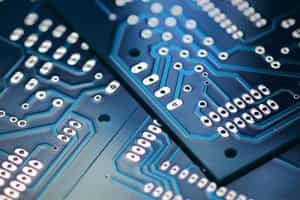
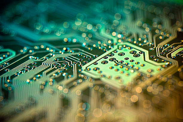
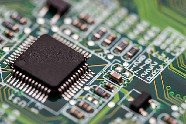
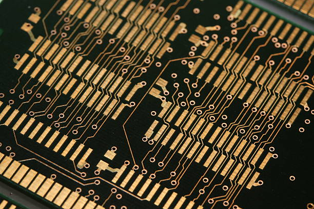
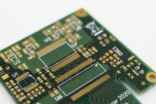
Double-sided PCB is the most used and preferred type of PCB because it is neither complex like a multilayer PCB nor simple like a single-layer PCB. It lies in between these two categories and is used in a wide range of applications.

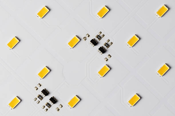
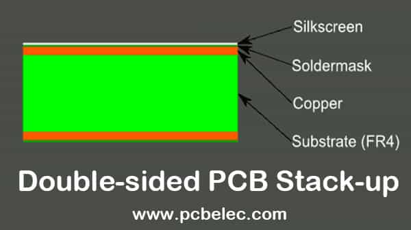
Double-sided PCBs have two layers, one on each side. The stack-up is quite simple as there are no inner layers. The components are placed on both sides of the PCB, which is why it is more compact than single-sided PCBs.

Double-sided PCB Stack-up

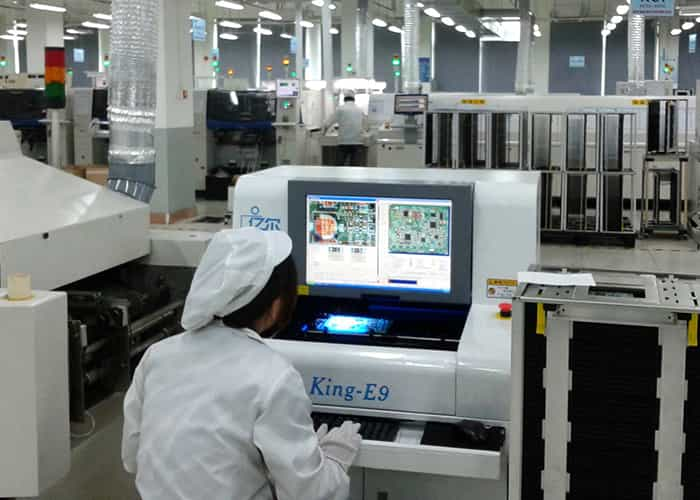
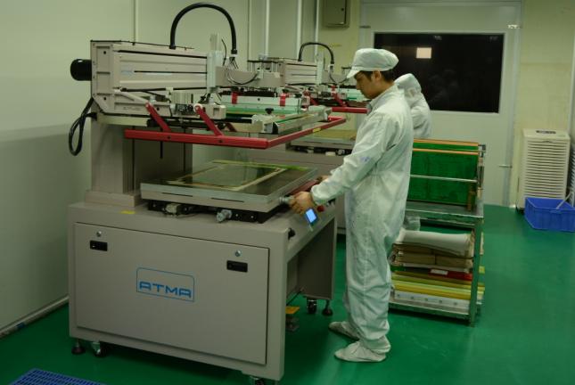
Even if you know how to design PCBs and are an expert, you need to understand the manufacturing process. Sometimes, the design is technically correct, but it can’t be achieved because of the limitations of the manufacturing process. Only the experts in the PCB industry understand the nitty-gritty, but designers should also have an idea of the whole manufacturing process.

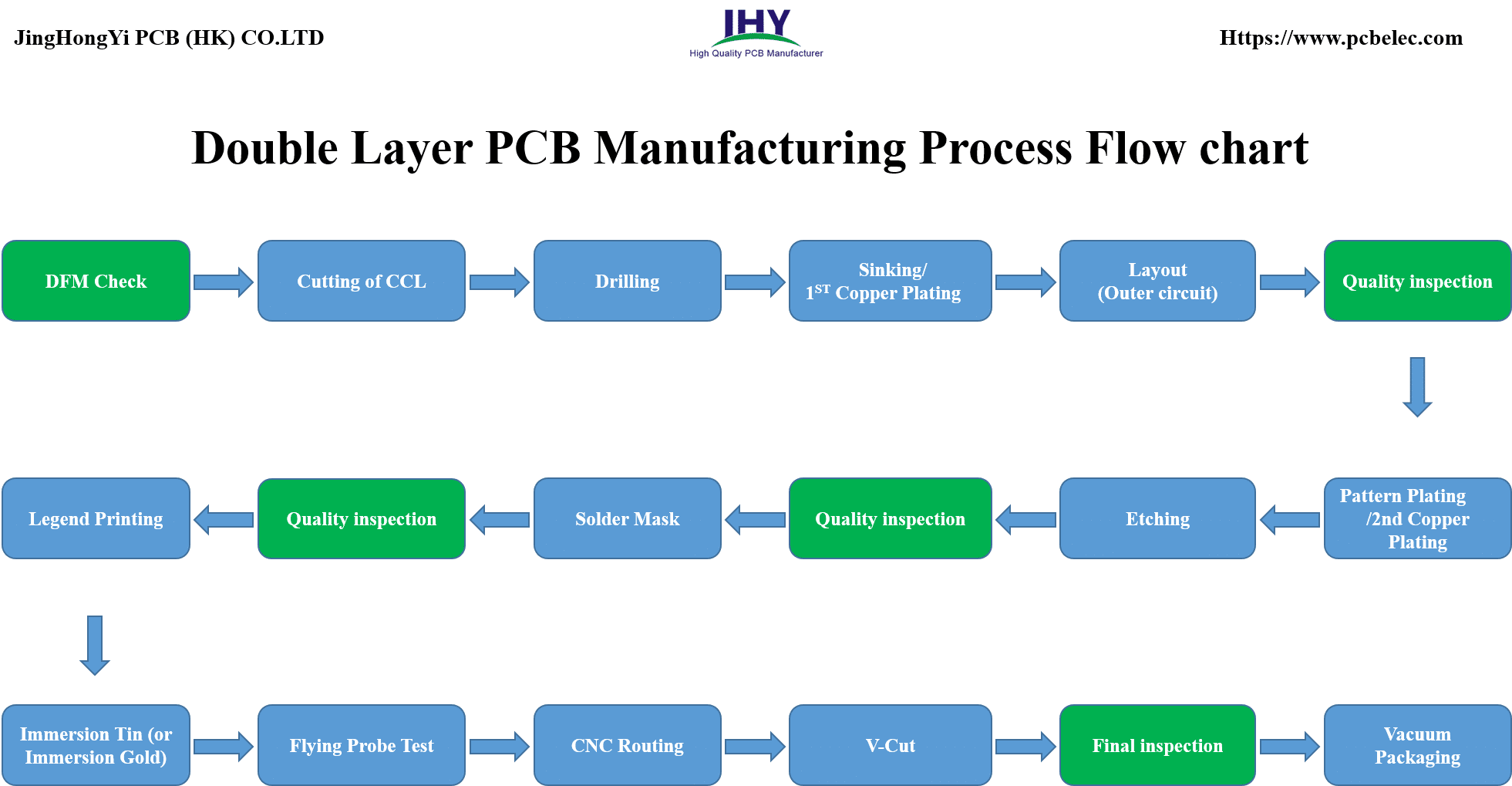
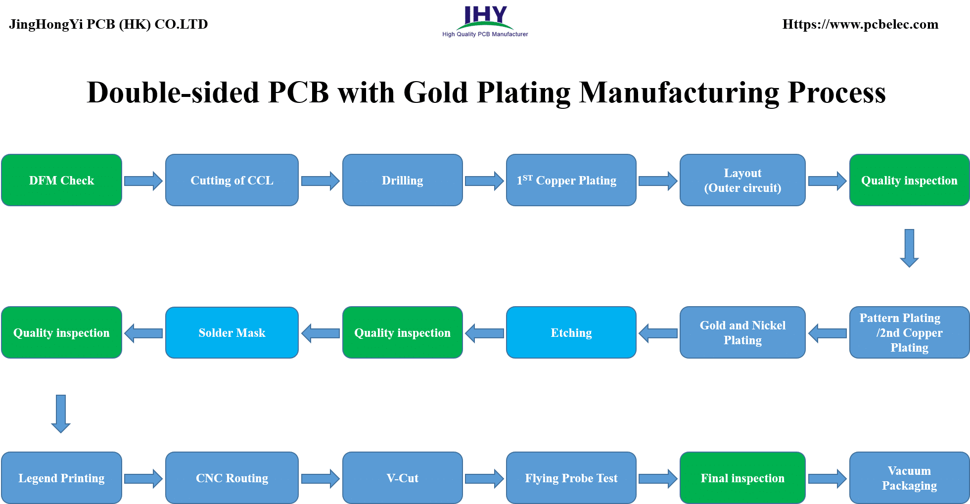
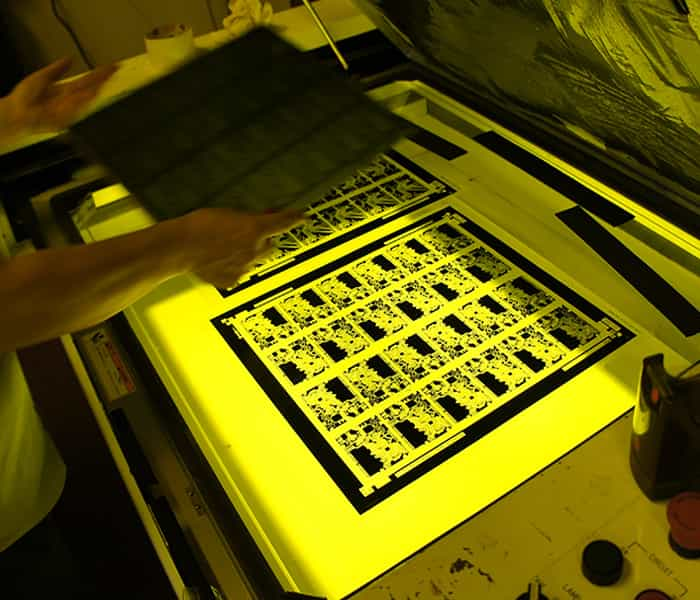
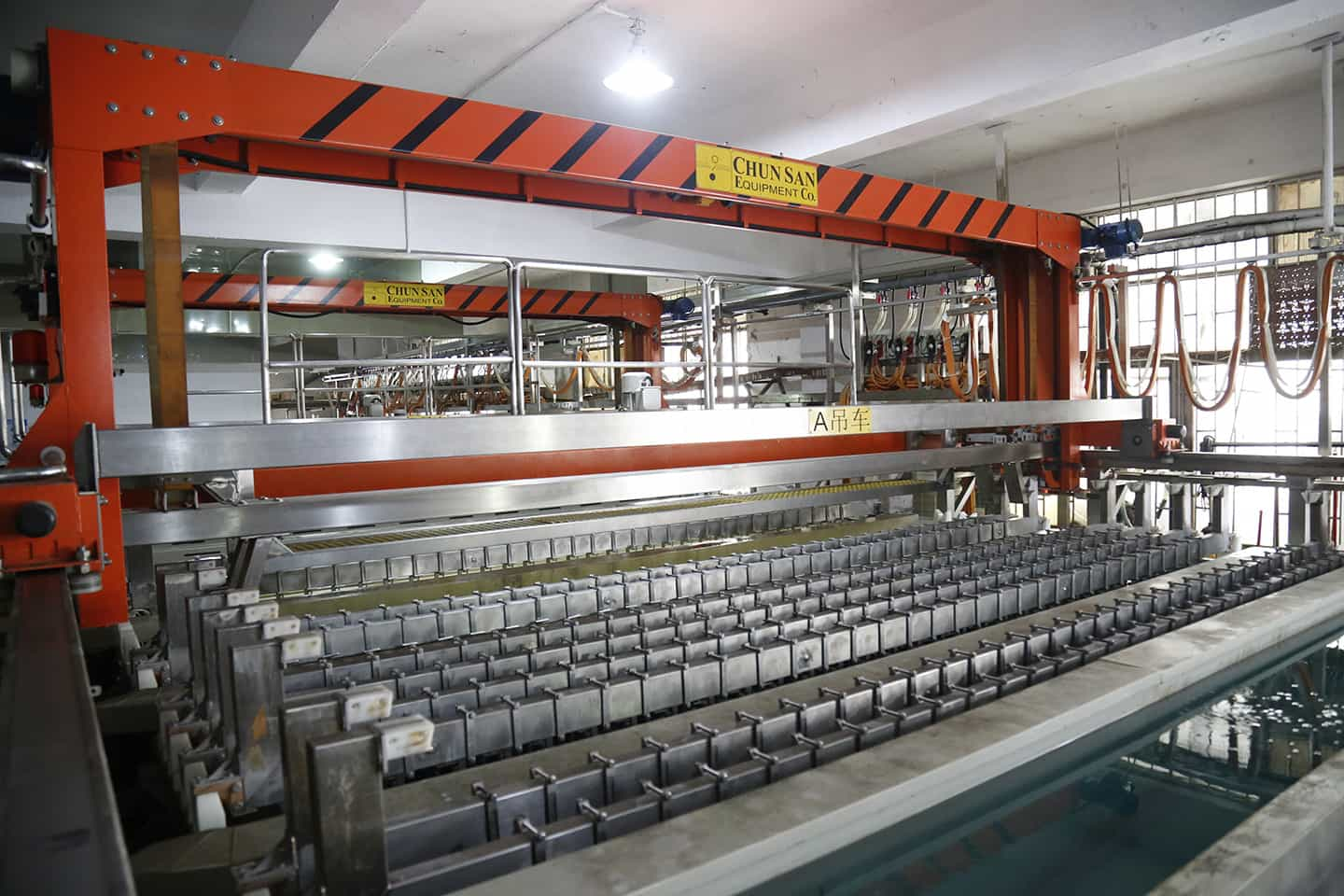
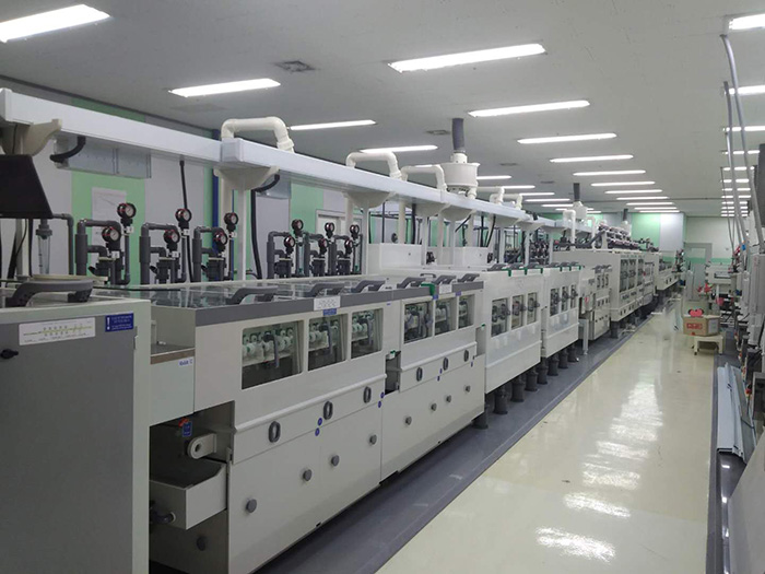
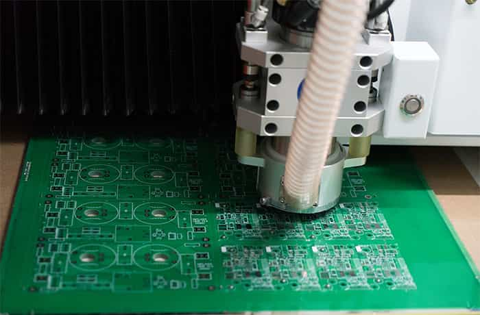
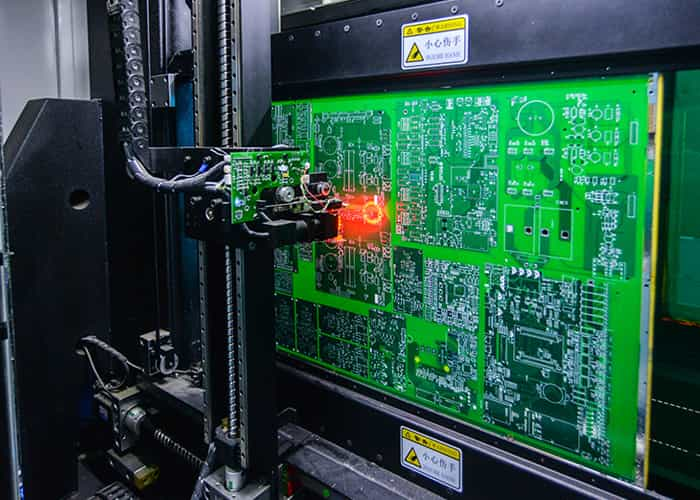
In this article, we will explain every step involved in the manufacturing of double-sided PCBs. There is little difference between the manufacturing process of single-sided, double-sided, and multilayer PCBs, but here, we will focus on double-sided PCBs.

How to Make a Double-sided PCB?

Double-sided PCB
Double Sided PCB Fabrication Process

Double Layer PCB Manufacturing Process Flow chart

Double Layer PCB With HASL-LF / Immersion Gold Surface Finish Manufacturing Process And Flow Chart

DFM Check—> Cutting of CCL—> Drilling —> Sinking/1ST Copper Plating —> Layout  (Outer circuit) —>Quality inspection—> Pattern Plating/2nd Copper Plating —> Etching —> Quality inspection—>Solder Mask —> Quality inspection—>Legend Printing —>Immersion Tin (or Immersion Gold) —> Flying Probe Test —> CNC Routing —> V-Cut (some boards do not need this) —> Final inspection—> Vacuum Packaging

Double-Layer PCB Manufacturing Process Flow Chart

Double-sided PCB with Gold Plating Manufacturing Process And Flow Chart

DFM Check —> Cutting of CCL —> Drilling —> 1ST Copper Plating —> Layout (Outer circuit) —>Quality inspection—> Pattern Plating/2nd Copper Plating —> Gold and Nickel Plating —> Etching —> Quality inspection—>  Solder Mask —> Quality inspection—> Legend Printing —> CNC Routing —> V-Cut —> Flying Probe Test —> Final inspection—> Vacuum Packaging

Double-sided PCB with Gold Plating Manufacturing Process
The Complete Manufacturing Steps Of Double Sided PCB

The Double-sided PCB Manufacturing Process Step by Step

PCB manufacturing is a complex process. The raw board goes through various steps, and at last, we have a double-sided PCB. We will take you through each step in this article. We will try to explain everything you should know about the manufacturing process.

Step 1: PCB Circuit Design

The first step before PCB design and manufacturing is to design the schematic diagram. We have a lot of PCB design software chosen. For example, here, we list more than 30 PCB design software for free download. However, based on our experience, EDA and Eagle are recommended.

Step 2: PCB Layout Design

After the PCB schematic design is completed, you can now start the PCB layout design. The tools we need to use include the Eagle EDA. Then use a laser printer to print the PCB layout on glossy paper.

Remember, Before top layer printing,You need to mirror the image of the top layer layout. Otherwise, The circuit will be inverted.

Step 3: DFM Check

The process starts from checking the file that the customers have sent. The designs and files received are usually made by an engineer, and it is quite common that the engineer might not be familiar with the manufacturing process, limitations, and other issues.

Most of the time, the designers create files according to their needs, and the files/designs don’t comply with the manufacturing processes. It is a severe issue that can lead to delays and problems while manufacturing the PCB. Thus, it is crucial to ensure that everything is according to the manufacturing process.

This checking is known as DFM check, which means Design for Manufacturability. The experts look at the file and rectify the flaws and issues. They look at the traces, layers, holes, pads, and everything to ensure the design is perfectly ready for manufacturing. Once the design and files are ready, they are sent for the manufacturing of the circuit board.

Step 4: Selection of PCB materials

There are a lot of materials used in PCB manufacturing for users and PCB manufacturers to choose from. Different brands and materials have different characteristics, and different materials also provide different benefits, such as FR4, a ceramic substrate, iron substrate, aluminum substrate, etc.

Fr-4, one of the flame retardant materials widely used in PCB base substrates. FR4 board is economical and affordable and can maintain the stability and safety of the PCB board under extreme temperature conditions.

However, FR4 is not suitable for high-frequency and high-speed PCBs. At this time, we need to choose high-frequency materials, such as Rogers’ RO4000 series, RT5000/6000 series, Tacanic’s TLX series, and so on.

We use aluminum, metal, or copper as the substrate for LED PCB or aluminum PCB used in the LED lighting industry.

Copper clad laminate storage room in PCB Factory

Copper-clad laminate is one of the most important raw materials for circuit board manufacturing.

Step 5: Cutting of CCL(Copper Clad Laminate)

The next step is to cut the board according to the requirement. The raw PCB board is quite large. There are various sizes available, such as 37 x 49 inches, 41 x 49 inches, and 43 x 49 inches. Therefore, it is cut in the required sizes that can be used in the machines.

Keep in mind that the board size obtained after cutting is not according to your circuit size; it is much larger than that. Your PCB size could be small, so multiple circuits on the board can make the process economical.

For instance, if you have ordered five PCBs of 4 x 4 inches, there will be much space left on the board after accompanying all your five PCBs. Thus, circuits of other customers are also placed on the same board, and after manufacturing, the circuits are cut and separated from each other. The idea is to use the board space wisely and accommodate as many boards as possible. It makes the process more economical.

After cutting the board, the sides are made smooth, and the edges are trimmed. The board has copper layers on both sides, so it is suitable for creating a double-sided PCB.

Cutting machine

Cutting Machine

Step 6: Drilling

The circuit board goes to an automatic drilling machine that creates holes in the board quickly. The machine changes the drill bits on its own; everything is automated.

Drill holes play various roles on a circuit. The simplest type of hole is the mechanical hole, which is made at the edges of the board. This type of hole is for holding the circuit board using screws.

There are three crucial holes done on a PCB, and they are known as vias. The first one is the Plated Through Hole (PTH), which creates a hole from one end of the PCB to the other. You can see from the hole. This type of hole is used to connect the components. It also connects inner layers, but in the case of double-sided PCBs, there is no inner layer.

The other two types of vias are blind and buried vias. These vias join the inner layers, and there is no need for these in double-sided boards.

After drilling, the board passed through a cleaning chamber to remove the dirt and debris. Then, the holes are plated from the inner side with copper. First, a thin copper layer is applied, and then the board goes through electroplating to increase the thickness of the copper in holes.

PCB drilling workshop
Finished drilled plates that have been cleaned and deburred

Step 7: Electroless copper deposition - Plating Through Holes

Electroless deposition of Cu through the holes as holes are composed of epoxy initially. After Cu deposition, panel is dipped in acid dip and anti-tarnish solution to prevent against oxidation. It is of two types- horizontal and vertical. Horizontal PTH is for carbon deposition and vertical PTH is for Cu deposition.

Electroless copper is one of the most important steps in double-sided PCB and multilayer PCB manufacturing processes. Because all PCBs with 2 or more layers use use plated through holes to connect the conductors between the layers.

Electroless copper deposition - Plating Through Holes

Step 8: Photo Imaging and Printing of Circuit

In this process, a film is created that has the circuit design. It is used to transfer the circuit design on the PCB board.

A photoresistive film is applied on the board obtained from the previous. The film is hot rolled on the board using a machine. Once the film is applied, the board is ready to be exposed to UV light for circuit printing.

The whole process is carried out in a room where there are only yellow lights. It is because photoresistive films are sensitive to other lights. Moreover, the person working inside the area wears a special suit and passes through a dust and dirt cleaning chamber before entering the room.

The film that has the circuit design is applied over the board; it is applied on both sides. Then, the board passes through a UV light chamber. When the board is exposed to UV light, the circuit part is hardened, while the excessive part remains the same. You can see the circuit design on the board.

Photo Imaging and Printing of Circuit

Step 9: Pattern plating

The thickness of copper on the PCB surface is specified by the customer. The copper surface of the panels is cleaned and activated in a number of baths and then electroplated. The whole process is computer controlled to ensure that each set or flight of panels stays in each bath exactly the right amount of time. You can see the copper anodes in their bags.

After copper plating, tin is plated on the copper laminate as the anode, and the PCB board acts as the cathode for electroplating, and then electrolysis is carried out.

To ensure good conductivity through the holes we need to plate an average of 20 microns of copper on the hole walls (18 µm copper is the defined minimum in the IPC 600J-Class 2 standard). This means that we also plate +/- 20 microns on the surface tracks.

The baths are designed to produce an even copper thickness across the panel. Modern chemical solutions also have good “throwing power” to produce an even thickness of copper right through the hole.

Once we have plated the copper onto the board we then plate a thin layer of tin. This we will use in the next step of the process when we etch off the unwanted copper foil.

Pattern Plating

Step 10: Developing and Etching

Now the board is cleaned using a developing solution. It removes the unhardened photoresist from the board. After that, only the hardened part is left, which is the circuit pattern.

The raw board has copper on both sides, and it is spread all over the board. Thus, the whole surface is conductive. 

We only need the conductive part for the circuit, and the rest of the copper should be removed. For this, the board is passed through an etching solution. The solution takes out the excess copper from the board, and the copper under the hardened photoresist remains the same.

After etching, the hardened film is also removed by going through various washing chambers. The outcome of this step is a board that has a complete circuit on it. The copper is only on the circuit, and there is no extra copper. The circuit is almost ready.

Developing and Etching Machine

Step 11: Automatic Optical Inspection (AOI)

Before going further, the circuit must go through an inspection process to make sure everything is perfect. After etching, there are chances of open circuits, short circuits, or any other issues. So, it is essential to carry out an inspection before going further.

Automatic Optical Inspection is a simple test that takes images of the circuit board using cameras. The images are then compared with the original design. After comparison, the issues are detected, and the circuit board is separated from the lot.

The best thing about this inspection is its fast pace. The cameras take images from different angles, and the process takes a few seconds to check one piece of board.

AOI

Step 12: Solder Mask

You might have seen green, white, blue, and other colors on the circuit. This is known as a solder mask. It is a thin layer of polymer that works as an insulator between two conducting lines. It prevents the formation of short circuits. The mask is applied all over the board, and then it is dried.

Now, it is time to remove the excess solder mask that is over the circuit. A film that contains circuit patterns is applied over the board. Then the board goes through a UV chamber. The solder other than the circuit is hardened while the solder mask over the circuit remains the same. Finally, the solder mask over the circuit is cleaned.

Step 13: Silkscreen

The labels on the PCB are called silkscreens. These can be used to mark components and insert the logo. In this step, the PCB board enters into a giant printer that prints the labels on the board.

Silkscreens are available in various colors, such as red, blue, yellow, and black, but the standard color is white. 

PCB Factory Screen Printing

Step 14: Surface Finish

The copper on the board can undergo oxidation. It cannot last for a long time. Therefore, it is necessary to apply a surface finish over copper to protect it from oxidation.

There are many types of surface finishes available, and customers can pick according to their needs. You can choose HASL, OSP, ENIG, ENEG, ENEPIG, Immersion tin, Immersion silver, etc.

Step 15: Routing

We have already discussed that there are multiple circuits on a board, and in the last, a cutting machine cuts the circuits and makes them separate pieces.

PCB Routing

Step 16: Flying Probe Test

Testing is an integral part of PCB manufacturing as it ensures the board is working as it should. There can be short circuits, open circuits, or any other issues. Thus, it is essential to check the PCB before delivering it to the customer.

For this purpose, the Flying Probe Test is used. It is a simple test in which there are multiple probes. The probes are placed over the connections, and the current is passed through them. It checks whether the circuit is working as expected or not. For instance, if there is no connection between two paths, then the current should not pass if the probes are connected to them.

This is the last step of a double-sided PCB manufacturing process. After this step, the PCBs are packed and shipped to the customers.

Flying Probe Test
Double Sided PCB Manufacturer In China

JHYPCB – The Ultimate Solution to Your PCB Needs

JHYPCB is one of the leading PCB manufacturers based in China. We are capable of handling large to small volume orders in our facility. Our customers can order even one PCB for their needs. Our management system is according to international standards; we are ISO, UL, and RoHS compliant.

We deal with all types of PCBs, including single-sided, double-sided, multiplayer, rigid, flexible, rigid-flex, BGA, HDI PCBs. We offer turnkey assembly services and quick prototypes. Our experts understand the nitty-gritty of the subject, and they can help you achieve your desired results from PCBs. Moreover, we offer the cheapest rate and quick delivery services.

For more information and details, feel free to contact our customer support.

Related Double-sided PCB manufacturing videos

Play Video about Double Sided PCB Prototyping

PCB Making – Double-layer PCB Prototyping

Play Video about Double Sided PCB Home Made DIY

Double Sided PCB Home Made DIY

Scroll to Top