
Flying Probe Testing for PCB
Flying probe testing is a method for low-volume and for prototype circuit boards.
Excellent electronic manufacturing service (EMS) providers or PCB assembly manufacturers should apply the best technology to provide customers with the best quality products and services.
Home » PCB Board Testing and Inspection » Flying Probe Testing for PCB
Printed Circuit Boards (PCBs) contain complex and compact circuits that may have some errors, such as short circuits, open circuits, diode issues, and bad solder. All these problems are not easily visible through the naked eye. Some PCB manufacturers do the manual inspection, but flying proper testing is necessary. There are various tests used to ensure the performance of PCB and find out possible faults. One of the most preferred tests is Flying Probe Testing (FPT).
What is Flying Probe Testing?
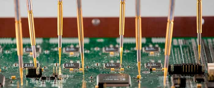
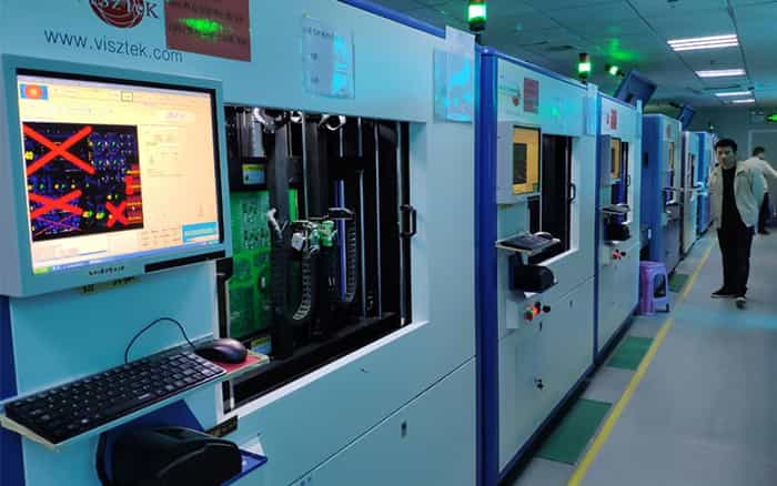
Flying Probe Testing is a test in which several probes move from one node/pad to another node/pad to check the PCB or PCBA. The probes move here and there, and it looks like they are flying from one place to another; therefore, this test is known as the flying probe test.
You might have heard a lot about ICT (In-circuit Testing). ICT works similarly to the FPT because it also tests PCB by placing the pins at the test points. However, it requires a special fixture that contains pogo pins to test the PCB. The fixture is commonly known as the bed of nails because it contains too many pins that resemble the nails’ actual bed. The PCB is placed on that fixture, and it is tested for defects. In contrast, the flying probe test does not require any fixture; therefore, it is also called fixtureless ICT. It has probes that move over the PCB from one node to another node.
At first, the flying probe test was only used to test the bare board (board without components). After some technological advancements, now the test is used for bare boards as well as assembled PCBs. It can detect short circuits, open circuits, wrong component placement, reverse polarity, and failure.
Flying probe testing is usually preferred for prototype, small-volume, and PCB assembly. It is cost-effective and convenient for small batches of PCBs. All PCB manufacturers use this method to detect the faults in PCBs and the finished assemblies.
How does Flying Probe Tester Work?
The working of the flying probe tester is extremely simple. It is almost like testing, checking component value, and measuring the resistance using a multimeter. The probes in the flying probe tester check each and every point on the board and ensure the board’s expected working and the components.
At first, a test program is created, containing all information about PCB, components, and test points. The plan directs the machine to the locations where it needs to place the probe for testing.
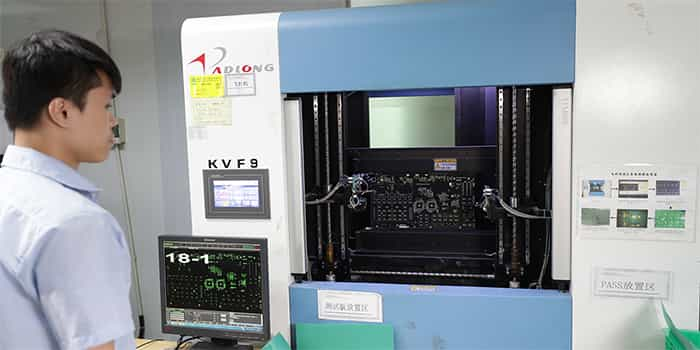
After creating the program, it is loaded into the flying probe tester. The PCB is placed on the conveyor belt. When the PCB comes under the tester, the test starts. The tester tests the PCB according to the program loaded in it. It applies different signals on the board to check the working of the components and detect any fault. It collects all the information about the PCB, and it compares it with the benchmark information. This way, it gets to know whether the PCB, any path, or component is delivering the desired results or not.
Flying probe testers can be used on PCB and PCB assemblies. In bare PCBs, it checks the short circuits and open circuits by checking the resistance between the paths. If there is any fault in the PCB, it is detected at this stage.
In assembled PCBs, the flying probe tester uses various electrical signals to check the working of the components. It also checks the value of the components; if there is any wrong placement or faulty component, the tester detects it. The testing machine can also check the polarity of the components.
The Function of the Electrical Test for PCBs
Advantages of Flying Probe Test
The first advantage of the flying probe is that it does not require any fixture. It does not require a bed of nails. It can work on any type of PCB, even on complex PCBs without the need for a fixture. There are a few probes in the tester, and they work according to the program loaded on the machine. The probes move from one test pad to another to carry out the test.
Since there is no fixture required, the cost of the fixture is eliminated. Moreover, there is no need to wait to start the test; you only need to create the program, and you are good to go.
Flying probe testing is cost-effective for small-medium volume production of PCB and PCBA. The prototype PCBs are also tested using this method. Even if there is only one PCB, this method can be used. It has less cost because it does not require any fixture. It saves time as it can be started whenever required.
The flying probe test can detect different types of faults, including open circuits, short circuits, wrong component placement, unexpected outputs of the component, fault in the component, tolerance, etc. So, it is an all-in-one test that can eliminate almost all kinds of major issues with the PCB.
The best thing about the flying probe test is its flexibility. Its program can be changed and amended when required. The program can be designed for any type of PCB. So, it offers maximum flexibility to the PCB manufacturers. Moreover, creating the test program is not a big deal, and it does not require too much time.
There is no need to dedicate separate test pads on the PCB. The flying probe test will utilize the existing pads of the PCB for testing.
Disadvantages of Flying Probe Test
- Slow and Expensive for High-volume Production
In flying probe testing, the probes test different pads one by one. So, it requires some time to test the complete board. The time depends on the size of the board; if the board is large, it will require more time. Therefore, this method is not suitable for high-volume PCB production. It will take too much time for testing. Moreover, it is also expensive for large volumes because other methods have a lower cost per unit.
- Cannot Test Components Simultaneously
FPT tests all components on the board, but it does test all components together. It might test the individual performance of the components; however, it cannot predict the overall result and performance.
ICT Testing vs. Flying Probe Testing-Which Suits Your Project?
People usually think of whether they should use ICT or FPT (Flying Probe Test) for your project. If you want to select the best one, you need to look at some important factors.
- The volume of PCB Production
The first thing that you need to consider is the volume of PCB or PCBA you need. If you are planning for high-volume production, ICT will be cost-effective. The cost per unit will be less than the cost of the flying probe test. But if you want low-medium volume production, ICT is not feasible. The upfront cost of ICT is a lot more than FPT. So, it is better to use the flying probe test in such cases.
In the case of PCB prototypes, the flying probe test is the only option because you cannot make a bed of nails fixtures for a few prototypes.
- Cost
You need to look at your budget. Flying probe test is efficient and cost-effective in low-medium production because it does not require any fixture. The cost of the fixture is several thousand dollars, which is actually a lot more than the programming cost of ICT and FPT.
The cost of creating a test program for ICT and FPT is almost equal, so you need to decide on the basis of whether the bed of nails fixture is cost-effective for your project or not.
- Time
ICT cannot be started soon because it requires a special fixture of nails that needs a few weeks to be created. So, ICT requires time. You need to understand the time required for this testing. On the other hand, the flying probe test can be quickly initiated because it does not require a fixture. As soon as the test program is ready, you can start the test.
No doubt that creating a fixture takes time, but once the fixture is created, the time required for testing is much less in ICT. The fixture has many nails, and it can test the PCB within a few seconds. In contrast, the flying probe test has a few probes, and it requires a few minutes, depending on the size of the PCB.
- Optical Inspection
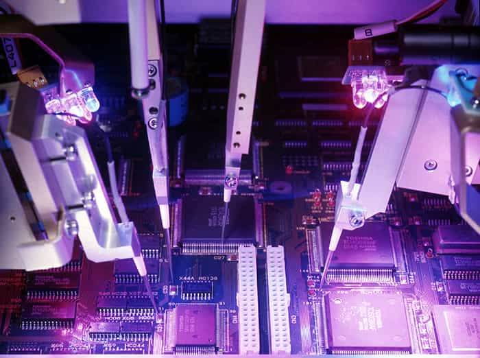
Optical inspection is necessary for polar components because their polarity cannot be checked using electrical signals. The flying probe test has the advantage of optical inspection. It can check the polarity of different components and ensure everything is perfect. This is not possible in ICT.
JHYPCB: You One Step Testing Solution
JHYPCB is a leading manufacturer and fabricator of PCBs and PCB assemblies. You will get a solution to all your PCB problems under a roof. We offer all types of PCB testing, including flying probe test, ICT, impedance test, voltage test, reliability test, slice analysis, AOI, X-ray inspection, laser inspection, and Hi-Pot PCB testing. Our company is certified by UL, RoHS, and ISO. Our strict quality management system ensures high-quality PCBs. For more information and details, feel free to contact us.
Related articles
- Testing & Inspection Methods For PCB And PCBA
- How To Testing A PCB For Short Circuit?
- What does PCB open Circuit Mean?
- What Is FR-4 Material In PCB Fabrication?
- The Difference Between Gold Plating and Immersion Gold
- Key Process Flow of Rigid-Fled PCB Production
- How to Store PCB and PCBA?
- How long can PCBA finished products be stored?
- Find Out Now, What Should You Do For Fast PCB Classification?