
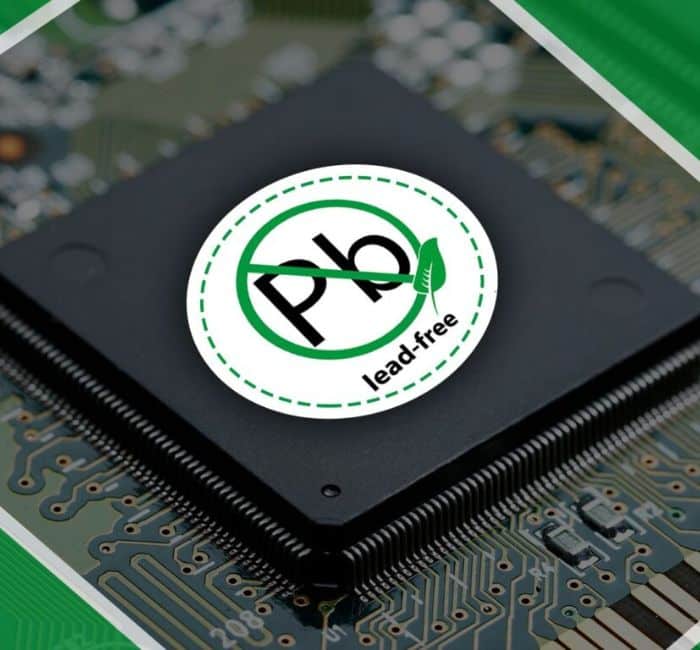
Lead-free PCB Assembly Service
JHYPCB offers reliable, cost-effective lead-free PCB assembly services. Our RoHS-compliant, green manufacturing process ensures high-quality, environmentally friendly PCB assemblies. Expertise in SMT, through-hole, quick-turn, and turnkey lead-free PCB solutions.
Home » PCB Assembly » Lead-free PCB Assembly Service
JHYPCB: Your Trusted Partner for Environmentally Friendly PCB Manufacturing
At JHYPCB, we pride ourselves on being a manufacturer of lead-free PCB assembly, offering environmentally friendly and RoHS-compliant PCB fabrication and assembly services. With years of expertise, we’ve perfected the art of lead-free manufacturing to ensure high-quality, reliable, and cost-effective products.
Our meticulous lead-free assembly process employs cutting-edge equipment and techniques. We use rigorously tested, high-performance lead-free solder pastes and materials that meet stringent standards. By eliminating hazardous lead, we contribute to a cleaner future while complying with environmental regulations.
The Lead-Free PCB Assembly Process
Our lead-free PCB assembly process is a meticulously controlled operation, leveraging state-of-the-art equipment and cutting-edge techniques. We employ only the finest lead-free solder pastes and materials, rigorously tested for superior performance, reliability, and compatibility with our stringent quality standards.
The process begins with thorough cleaning and preparation of the PCB surfaces, ensuring optimal adhesion and reliability of the lead-free solder joints.
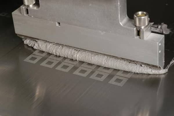
Using advanced stencil printers, we precisely apply lead-free solder paste onto the PCB pads, guaranteeing accurate and consistent deposition.
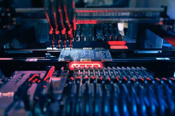
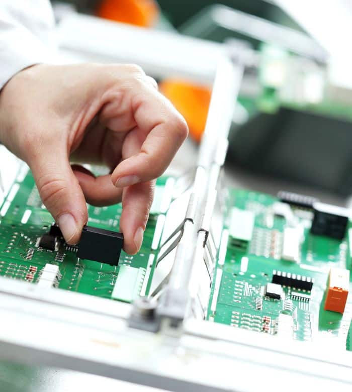
Our state-of-the-art pick-and-place machines carefully position the components onto the PCB, aligning them with the solder paste deposits for a perfect fit.
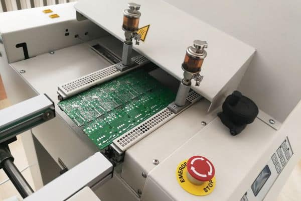
The assembled PCBs undergo a tightly controlled reflow soldering process within specialized lead-free ovens, using our advanced lead-free solder alloys. These alloys are specifically formulated with exceptional wetting abilities, high reliability, and oxidation resistance, ensuring robust and long-lasting solder joints.
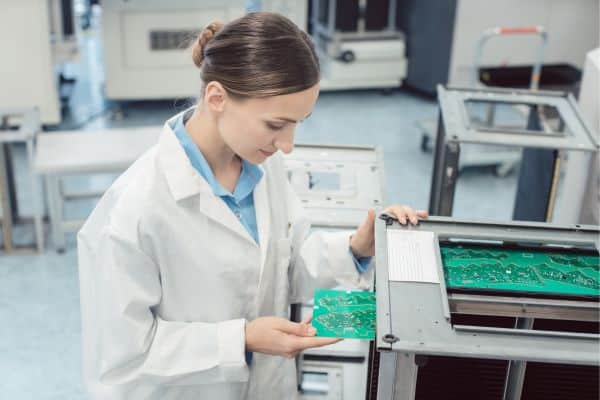
Quality control is paramount in our process. We employ advanced AOI systems and electrical testing to meticulously examine every lead-free PCB assembly for defects or issues. Our quality management system utilizes statistical process control with continuous monitoring and data analysis to maintain consistent quality and drive process improvements.
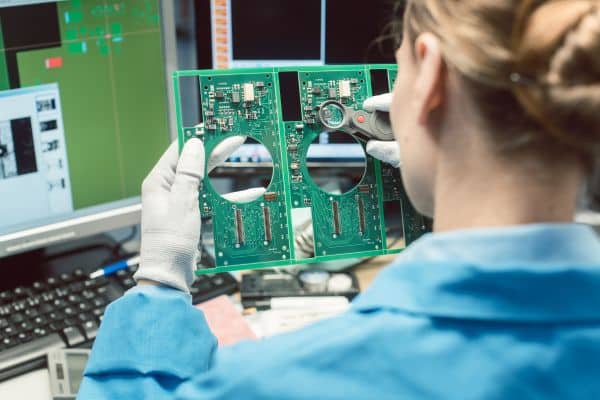
Before delivery, each lead-free PCB assembly undergoes a comprehensive final visual inspection by our highly trained technicians, ensuring adherence to our strict acceptance criteria and customer requirements.
Throughout the assembly process, we maintain strict control over every parameter, including temperature profiles, atmosphere conditions, and material handling. Our state-of-the-art equipment and rigorous process controls ensure repeatable quality and minimize defects in our lead-free PCB assemblies.
By combining cutting-edge lead-free materials, advanced assembly techniques, and stringent quality practices, we deliver superior lead-free PCB products that meet the highest standards of performance, reliability, and environmental sustainability.
Lead-Free PCB Assembly Capabilities
At JHYPCB, we offer comprehensive lead-free PCB assembly services, catering to a diverse range of customer requirements. Our state-of-the-art facilities and experienced team enable us to handle projects of varying complexities, from simple to highly intricate designs.
Our lead-free assembly expertise extends to various PCB types, including rigid, flex, rigid-flex, and HDI boards. We can accommodate projects with board sizes ranging from small and compact to large and complex layouts, ensuring efficient and precise assembly for each unique application.
We excel in both lead-free surface mount technology assembly and through-hole assembly processes. Our advanced SMT lines are equipped with high-precision pick-and-place machines capable of handling even the smallest components, while our through-hole assembly capabilities allow for reliable lead-free soldering of through-hole components.
Understanding the importance of time-to-market, we pride ourselves on offering rapid lead-free PCB assembly services with flexible production schedules. Our streamlined processes and efficient operations enable us to deliver high-quality assemblies with industry-leading turnaround times, ensuring your products reach the market swiftly.
Quality Assurance
At JHYPCB, quality is deeply ingrained in every aspect of our lead-free PCB assembly operations. We adhere to stringent quality management systems and industry-leading practices to ensure consistent and reliable results.
Our comprehensive quality control process encompasses multiple stages, from incoming material inspection to in-process monitoring and final product testing. We employ advanced inspection techniques, including AOI and electrical testing, to identify and eliminate any potential defects or non-conformances.
Our lead-free PCB assembly services are backed by various internationally recognized certifications, such as ISO 9001, ISO 14001, and IATF 16949, ensuring compliance with industry standards and customer requirements. Our lead-free processes are fully RoHS-compliant, demonstrating our commitment to environmental sustainability.
Environmental Stewardship
At JHYPCB, we are committed to minimizing our environmental impact and promoting sustainable practices throughout our operations. Our lead-free PCB assembly services are a testament to our dedication to environmental stewardship.
- Benefits of Lead-Free Assembly: By eliminating the use of hazardous lead-based materials, our lead-free PCB assembly process significantly reduces the environmental footprint of electronic products. This approach not only complies with RoHS and other environmental regulations but also contributes to a greener and healthier planet for future generations.
- Green Initiatives: Our commitment to environmental responsibility extends beyond lead-free assembly. We actively implement eco-friendly practices, such as energy-efficient manufacturing processes, responsible waste management, and the use of recyclable materials whenever possible. These initiatives reflect our dedication to sustainable operations and minimizing our carbon footprint.
Pricing and Ordering
At JHYPCB, we strive to offer competitive pricing for our lead-free PCB assembly services without compromising on quality or reliability. Our streamlined processes and efficient operations enable us to provide cost-effective solutions tailored to your specific requirements.
To receive a detailed quote for your lead-free PCB assembly project, simply contact our knowledgeable sales team. They will work closely with you to understand your requirements, provide accurate pricing information, and guide you through the entire ordering process.
Once your order is placed, our dedicated production team will ensure a smooth and efficient assembly process. We maintain transparent communication throughout, keeping you informed about the project’s progress and adhering to agreed-upon lead times for delivery.
Our commitment to customer satisfaction extends beyond the initial assembly process. Our skilled support team is available to address any inquiries, provide technical assistance, and ensure your complete satisfaction with our lead-free PCB assembly services.
About JHYPCB
JHYPCB is a leading PCB manufacturer and solution provider, offering a comprehensive range of services, including lead-free PCB assembly, SMT, and through-hole assembly. With years of industry experience and a team of highly skilled professionals, we have built a reputation for excellence, reliability, and customer satisfaction.
Our core values revolve around quality, innovation, and environmental responsibility. We continuously invest in state-of-the-art equipment and technologies to stay at the forefront of the industry, ensuring we deliver cutting-edge solutions to our valued customers.
At JHYPCB, we pride ourselves on our commitment to building long-lasting partnerships with our clients. Our dedicated customer support team is always ready to assist you, providing personalized solutions and ensuring your projects are executed flawlessly.
For inquiries, quotes, or further information about our lead-free PCB assembly services, please contact us through our website or reach out to our knowledgeable representatives.
Experience the JHYPCB difference – where quality, reliability, and environmental stewardship converge to deliver exceptional lead-free PCB assembly solutions tailored to your unique needs.
Frequently Asked Questions
Lead-free PCB assembly refers to the process of manufacturing printed circuit boards and assembling electronic components without the use of lead-based materials, in compliance with regulations such as RoHS and REACH. According to these regulations, the lead content of solder paste used for PCB assembly must be within 0.1%.
For a truly lead-free PCB assembly process, the lead-free requirement (Pb < 0.1%) extends throughout the entire EMS manufacturing process. This includes electronic components, PCB copper-clad laminates (CCL), PCB inks, surface finishes, solder paste, enclosures, packaging bags/boxes, and all equipment/devices/jigs used during the fabrication process.
By eliminating lead from the assembly process, lead-free PCBs minimize environmental impact and health risks associated with lead exposure, while still ensuring reliable and high-performance electronics.
For lead-free PCB assembly, there are several compatible surface finish options for printed circuit boards. These include:
- ENIG (Electroless Nickel Immersion Gold)
- OSP (Organic Solderability Preservative)
- ENEPIG (Electroless Nickel Electroless Palladium Immersion Gold)
- Lead-free HASL (Hot Air Solder Leveling)
- Gold plating
- Immersion silver
- Immersion tin
- Carbon ink
For flexible PCBs, lead-free HASL cannot be used, and OSP or ENIG finishes are recommended as alternatives.
The choice of surface finish depends on factors such as the PCB design, assembly process requirements, and end-use application. Proper surface finishes play a crucial role in ensuring reliable solder joint formation and long-term performance in lead-free PCB assemblies.
The lead-free solder paste used for PCB assembly is composed of Sn/Ag/Cu/Bi alloy powder and flux. It follows the RoHS directive and is typically packaged in green bottles. Solder paste is stored at temperatures between 2°C to 8°C and used at room temperatures ranging from 22°C to 28°C.
In the lead-free PCB assembly process, solder paste plays a crucial role. For OSP PCBs, the solder in the solder paste melts and forms metallic compounds with the copper pads. For PCBs with other surface finishes, such as ENIG or ENEPIG, the solder, surface finish, and copper pads form metallic compounds during the reflow process.
The flux component in the solder paste activates the solder and helps in the formation of reliable solder joints. After the reflow process, the flux typically evaporates, leaving behind the solidified solder joints.
Reflow soldering is the most critical step in the lead-free PCB assembly process. The reflow temperatures follow a specific lead-free reflow profile, which includes the preheat stage, soak stage, reflow stage, and cooling stage.
For lead-free FR4 PCBs, the peak temperature range during the reflow stage is typically between 240°C to 270°C. Compared to PCB assembly with lead-containing solder, the reflow soldering temperatures for lead-free assemblies are approximately 30°C higher.
However, for thick-copper PCBs, heat transfer occurs rapidly, and the reflow temperatures need to be higher to ensure sufficient soldering of the tin alloy on the PCB pads. Based on our extensive experience, we set the peak reflow temperatures for thick-copper PCBs to be between 290°C and 300°C.
Precise control of reflow temperatures is crucial for achieving reliable solder joints and ensuring the long-term performance of lead-free PCB assemblies.
PCBA manufacturers are subject to RoHS standards, which require replacing traditional lead-based solders with lead-free alternatives for RoHS-compliant PCB assembly. You may benefit from using lead-free PCB assembly in the following situations:
- Your products will be sold in countries or territories with regulatory requirements for lead-free electronics, such as the European Union.
- Your state or local government mandates lead-free manufacturing processes, such as in California.
- You are concerned about potential health risks associated with the use of lead-based products.
- You want to mitigate potential liability risks associated with products containing lead.
- You recognize the growing demand for green manufacturing practices and want to attract environmentally conscious customers.
- You understand the advancements lead-free PCB assembly has brought to small-volume PCBA manufacturing and want to promote continued innovation in this area.
By adopting lead-free PCB assembly, manufacturers can comply with regulations, address environmental concerns, and meet the evolving needs of customers who prioritize sustainability and responsible manufacturing practices.
There are several notable differences between traditional leaded PCB assembly and lead-free (RoHS-compliant) PCB assembly:
- Environmental Impact: The most significant difference is environmental protection. Leaded solder paste contains lead (Pb), which is highly toxic to human health and the environment. Lead-free soldering eliminates the use of hazardous lead, making it an environmentally friendly option.
- Solder Alloy Composition: Leaded solder typically consists of 60% tin and 40% lead. In contrast, the most widely used lead-free solder alloy is SAC305, comprising 96.5% tin, 3% silver, and 0.5% copper. While lead-free processes cannot be 100% lead-free, the lead content should be less than 1000 ppm (<0.1%) to comply with RoHS and REACH regulations.
- Melting and Operating Temperatures: Leaded solder has a melting point of 180°C to 190°C and an operating temperature of approximately 240°C to 260°C. Lead-free solders have higher melting points, typically ranging from 210°C to 230°C, with operating temperatures between 250°C and 280°C. However, low-temperature lead-free solders melting below 200°C have been developed.
- Cost: Lead-free solder and the associated assembly process are generally more expensive than their leaded counterparts. This is primarily due to the higher cost of the base materials used in lead-free solder alloys.
It’s important to note that the transition to lead-free PCB assembly has been driven by environmental regulations and concerns, aiming to reduce the impact of hazardous substances on human health and the environment.
Lead-free PCB assembly offers several advantages, including reduced environmental impact, compliance with RoHS and other environmental regulations, improved reliability and longevity of solder joints, and enhanced safety for both manufacturers and end-users.
Lead-free PCB assembly typically uses solder alloys that are free of lead, such as tin-silver-copper (SAC) alloys. Other materials may include lead-free surface finishes, fluxes, and conformal coatings designed for compatibility with lead-free processes.
Initially, lead-free assembly processes and materials may have been more costly. However, as the industry has transitioned to lead-free solutions, the costs have become more comparable, and the long-term benefits often outweigh any initial cost differences.
Yes, modern lead-free solder alloys and materials are designed to withstand high temperatures and thermal cycling, ensuring reliable performance in various operating environments.
Absolutely. Our state-of-the-art facilities and experienced team are equipped to handle lead-free PCB assembly projects of varying complexities, from simple designs to high-density interconnect (HDI) boards and other intricate layouts.
At JHYPCB, we pride ourselves on offering flexible production schedules and quick turnaround times for our lead-free PCB assembly services. Our streamlined processes and efficient operations enable us to deliver high-quality assemblies within industry-leading lead times.
The terms “lead-free PCB assembly” and “RoHS-compliant PCB assembly” essentially refer to the same thing – they both indicate that the assembled printed circuit boards are environmentally friendly and comply with relevant regulations.
Specifically, both terms imply that the PCB assembly process does not involve the use of lead (Pb) or other hazardous substances restricted by the RoHS (Restriction of Hazardous Substances) directive.
In a lead-free or RoHS-compliant PCB assembly, traditional lead-based solder is replaced with lead-free solder alloys, typically containing tin, silver, and copper. The lead content in the solder and other materials used in the assembly process must be below the maximum concentration value specified by the RoHS directive, which is currently 0.1% by weight.
By adopting lead-free or RoHS-compliant PCB assembly practices, manufacturers can ensure that their products meet environmental regulations, reduce potential health risks associated with lead exposure, and promote sustainability in the electronics industry.
In essence, both terms highlight the absence of lead and other restricted substances, making the assembled PCBs environmentally friendly and compliant with global environmental regulations.
Feel free to contact our knowledgeable team if you have any additional questions or concerns regarding our lead-free PCB assembly services.