
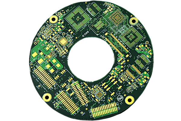
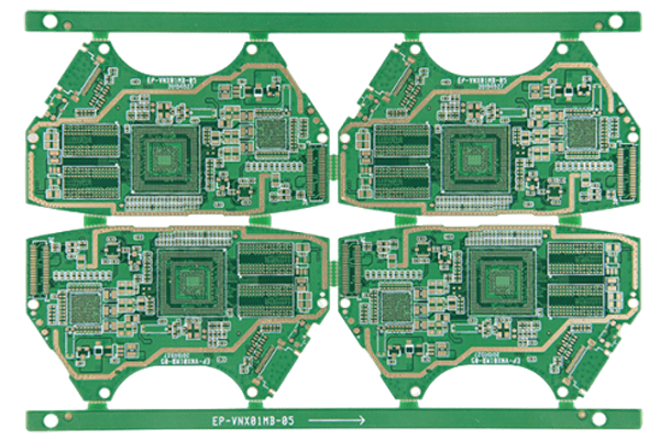
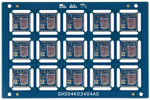
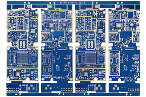
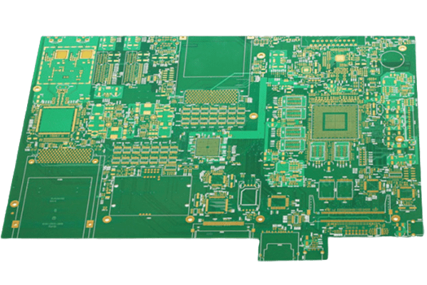
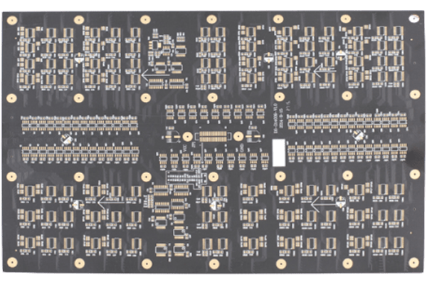
High Density Interconnect (HDI) PCB Board Manufacturing service
Home » PCB Manufacturing » HDI PCB
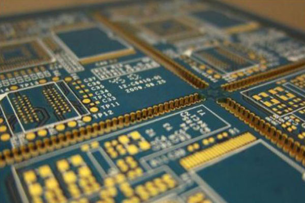
What is a HDI PCB ?
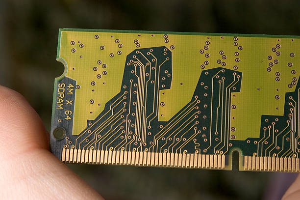
HDI stands for High-Density Interconnector. Thus, HDI PCB is a special type of PCB that has the capability of high-density interconnections. In simple words, it has more wires or conduction lines per unit area, utilizing the most out of the space and offering a compact PCB.
HDI PCBs VS. Conventional PCBs
Contrary to the conventional PCBs, this PCB has tightly packed interconnections; thus, it saves a lot of space and offers more component density. Suppose a conventional multilayer PCB has ten layers for the implementation of a circuit and is about 5 inches x 5 inches in dimension. The same circuit can be implemented on an HDI PCB, and there will be fewer layers, could be eight layers or fewer. Moreover, the size of the board will also reduce. Thus, HDI PCB has the capability of making a circuit compact.
The world is moving towards more and more compact devices, appliances, and equipment. Everything is getting smaller and smaller day by day, and an important role in this regard has been played by HDI PCB. It has helped in achieving smaller designs of the products, faster processing, and other benefits, but everything comes at a high cost. HDI PCBs are more costly compared to other boards because of their exceptional features.
How is High-Density Interconnection Achieved? - Microvias
Conventional multilayer PCBs require plated through-hole (PTH) vias to create a connection between the layers. The vias take more space, and if space requirement is reduced, we can easily achieve high-density interconnection.
HDI PCB promises a high density of interconnection in the given area. This is because it uses special blind and buried vias. It uses micro vias that are drilled using a laser. The diameter of the laser beam is 1 Mil, so it can create a tiny via to save space. Due to the use of laser technology, this type of via has a very small diameter, nearly 0.006 inches (1.5mm) or lesser than that. Consequently, there are few layers in the PCB, and high-density interconnection is achieved.
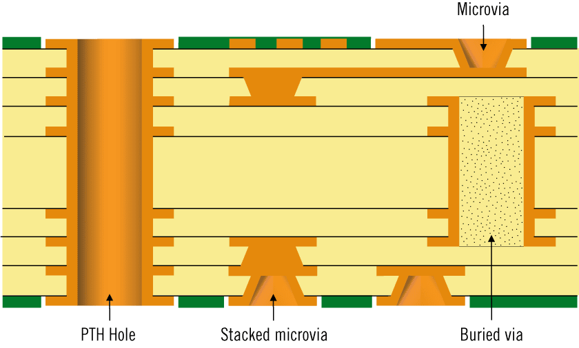
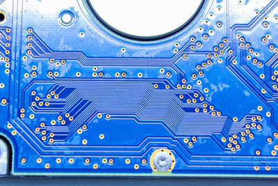
PTH Hole, Stacked Microvia, Buried Via, Microvia in HDI PCB Board
Micro vias are created with extra precision, and they are more accurate compared to mechanical drilling. Due to the presence of micro vias, there is more space available on the boards, so there are more pin counts on the PCB. This ensures the placement of more components compared to traditional PCBs. Along with the benefit of space-saving, micro vias also bring many advantages, including faster signal transmission, low resistance and capacitance, and reduction in the weight of the final PCB.
The most important thing about micro vias is that they can be placed inside the pads of the surface-mounted components. These vias are quite small, so they can utilize the space under the pads. These vias are known as microvias-in-pad. They save a lot of space on the PCB as there is no need for a separate space to create micro vias. They can even be placed under the pads of fine pitch BGA components/packages.
Mircovias can be classified into various types.
- Blind Micro vias: These vias start from the surface layer of the PCB and can connect several layers beneath it. It usually connects one or two layers to the surface layer.
- Buried Micro vias: These vias are inside the PCB, and they connect the internal layers of the PCB. They do not connect the surface layer to internal layers.
- Stacked Micro vias: The blind via can be stacked over a buried via. This is known as stacked micro via.
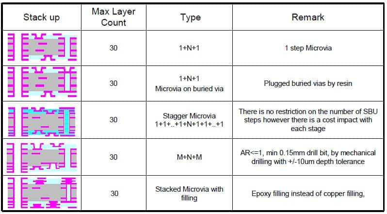
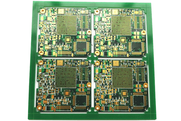
HDI PCB Builds
Depending on the design requirements, HDI Printed Circuit Boards can utilize different layering methods to achieve the desired performance.
HDI builds means how many times of laser drilling for microvias.
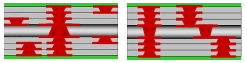
HDI PCBs are usually classified by the HDI builds, and there are the 1+N+1, 2+N+2, 3+N+3, 4+N+4, and 5+N+5. In the HDI PCB’s outer layers, micro vias usually form the more expensive stacked vias or cheaper staggered vias.
HDI PCB (1+N+1): Simplest HDI
- 1+N+1 is the simplest HDI build, and it means the HDI PCB’s microvias are single vias that need only one laser drilling.
- This structure of HDI PCB contains 1 “build-up” of high-density interconnection layers, suitable for BGA with lower I/O counts.
- It has fine lines, microvia and registration technologies capable of 0.4 mm ball pitch, excellent mounting stability and reliability, and may contain copper filled via.
- Applications: Cell phone, MP3 Player, GPS, Memory Card.
HDI PCB (2+N+2): Moderate Complex HDI
2+N+2 means the HDI PCB needs twice laser drilling, and both the upper and bottom outer layers have 2 PCB layers. Unlike 1+N+1, 2+N+2 has two cases. One is that the microvias of the two adjacent outer layers overlap, and the two microvia form a stacked via. The other case is that the microvias of the two adjacent outer layers do not overlap, and they form a staggered via. As we know, it requires extremely high precision to locate and pile up two microvias, so stacked via HDI PCBs are more expensive than staggered via HID PCBs.
- These are suitable for BGA with smaller ball pitch and higher I/O counts and can be used to increase routing density in a complicated design while maintaining a thin finished board thickness.
- Applications: Cell phone, PDA, game console, portable video recording devices.
HDI PCB (3+N+3)
3+N+3 means the HDI PCBs need three times of laser drilling and both the upper and bottom outer layers have 3 PCB layers.
ELIC (Every Layer Interconnection): Most Complex HDI
- In this HDI PCB structure, all the layers are high-density interconnection layers which allow the conductors on any layer of the PCB to be interconnected freely with copper filled stacked microvia structures.
- This provides a reliable interconnect solution for highly complex large pin-count devices, such as CPU and GPU chips utilized on handheld and mobile devices while producing superior electrical characteristics.
- Applications: Cell phone, ultra-mobile PC, MP3, GPS, Memory cards, small computer devices.
- The more times of laser drilling, the higher requirements for HDI PCB manufacturing technologies and more costs. 1+N+1, 2+N+2, 3+N+3, and 4+N+4 HDI PCBs are used commonly. 5+N+5 HDI PCBs are also in use but less.
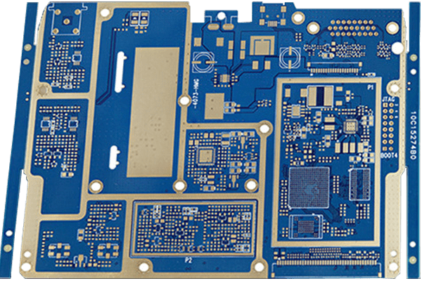
Applications of HDI PCB
HDI PCBs are widely used in modern devices and equipment because they are compact and offer excellent performance. These are used in mobile phones, wearable devices, MP3s, tablets, and other devices that tend to be compact.
These PCBs can be used in any application; however, the cost is much higher than conventional PCBs. There is no doubt that these PCBs offer exceptional benefits that other PCBs cannot provide, but they are mostly used at places where budget is not an issue. For instance, people pay higher prices for a slim and compact mobile phone, so HDI PCBs can be used in it.
Advantages of HDI PCB
- High Component Density
The first benefit of HDI PCB is that more components are placed in a small PCB board. It has a high component density. In conventional PCBs, space is taken by vias, especially PTH. But in HDI PCB, that space is utilized to have more connections and components.
- Space-saving
HDI PCBs use the space wisely. The vias are even placed under the pads of the BGA components and SMDs. A lot of space is saved, which is why the PCB is compact. It takes little space, and the final product is also compact.
- Fast Processing
HDI PCBs offer a high processing speed as the connections and components are very close together. The distance for signal transmission is reduced, so the resistance is also lower. The capacitance and inductance effects are also reduced. Thus, the signals move faster and improve the performance of the PCB.
- Lightweight Boards
The boards are lightweight as they are compact, and the circuit is much smaller than a conventional PCB. Thus, the final board is small and lightweight.
- Lower Number of Layers
The microvias reduce the number of layers in the PCB. In conventional multilayer PCBs, you need more layers, but the layers in HDI PCBs are less as space is perfectly utilized. The same result can be obtained in fewer layers and without compromising on the quality.
- Accommodate Low Pitch Packages
HDI PCBs are compatible with low pitch BGA components. They have more pin-outs, and due to microvias, they can easily accommodate low-pitch packages. SMDs can also be placed easily over the board.
- High Reliability
HDI PCBs offer high reliability as they have microvias. These vias provide the best performance in every condition. Moreover, the board can also bear high-temperature stress due to high TG.
Advanced PCB Materials for HDI PCB Fabrication
JHYPCB offers vast PCB material options for different applications from top manufacturers, such as Isola, Nelco, Arlon, Rogers, and Taconic. Our laminate options offer excellent properties that include:
- High Thermal Reliability
- Ultra-Low Loss
- High-Speed Digital
- Halogen-Free
- RoHS Compliant
- Lead-Free
- High Tg HDI Printed Circuit Board
Order High-Quality HDI PCBs from JHYPCB
JHYPCB offers high-quality HDI PCBs up to 30 layers. We can deal with small to medium HDI PCB orders without any restriction on the number of PCBs. Buyers can order PCB prototypes and assemblies with a fast turnaround. We offer quick turn prototypes and turnkey assembly services.
We ensure high-quality PCBs through strict quality checkups. We are certified by UL, ISO, and RoHS. Buyers can place their orders with confidence, and we promise to deliver PCBs in the shortest possible time and at cheap rates. For more information, quotes, and details, feel free to contact us.
Learn more about our HDI PCB Board Fabrication Capabilities