What is multilayer PCB?
PCB, or printed circuit board, is the mother of electronic products. The number of layers of the printed circuit board can be divided into single-sided PCB, double-sided PCB, and multilayer PCB.
Single-Sided PCB Boards
On the most straightforward PCB circuit board, the electronic components are concentrated on one side, and the circuits are on the other. Because the courses only appear on one side, this circuit board is called Single-sided PCB. Because single-layer PCB has many strict circuit designs (because there is only one side, the circuit cannot cross), only the first circuits use this type of board.
Double-Sided PCB Boards
There are circuits on both sides of a double-sided PCB, but for the circuits to work, there must be a proper circuit connection between the two sides of the circuit board. The “bridge” between such circuits is called a via. A via is a small hole filled or coated with metal on the PCB circuit board, connected to the course on both sides. Because the double board area is twice as large as the single-sided board, and because the circuit can be interleaved (it can be wound to the other side), it is more suitable for use in more complicated circuits than the single-sided PCB board.
Advanced Learning: Double-Sided PCB Manufacturing Process
Multi-Layer PCB Boards
As the name suggests, a multilayer circuit board can be called a multilayer circuit board with more than two layers, such as four, six, eight, and so on. Multilayer PCB circuit boards use more single-sided or double-sided circuit boards to increase circuit wiring. Use a double-sided board as the inner layer, two single-sided boards as the outer layer, two double-sided printed circuit boards as the inner layer, and two single-sided printed circuit boards as the outer layer. The positioning system and the insulating adhesive material alternately form a conductive pattern. According to design requirements, printed circuit boards become four-layer or six-layer printed circuit boards, also known as multilayer printed circuit boards. The number of layers of the circuit board means several independent wiring layers; usually, the number of layers is even and contains the two outermost layers. Most motherboards have a 4 to 8-layer structure, but it can be a PCB circuit board with nearly 100 layers in theory. Most large supercomputers use fairly multi-layered motherboards, but because clusters of many ordinary computers can already replace these types of computers, super-multilayered boards have gradually ceased to be used.
The advantage of the multilayer PCB circuit board is that the lines can be distributed in multiple layers to be designed more precisely. Or smaller products can be realized by multilayer boards, such as mobile phone circuit boards, micro projectors, voice recorders, and other products with relatively large volumes. Besides, multilayer can increase the flexibility of design, better control the differential impedance and single-ended impedance, and give some signal frequency better output.
Multilayer printed circuit boards are widely used to manufacture electronic products due to their flexible design, stable and reliable electrical performance, and excellent economic performance. Especially with the extensive and in-depth application of large-scale integrated circuits, multilayer PCBs are developing in the direction of high density, high precision, and high-level digitization. Fine lines, slight aperture penetration, and blind hole technologies (such as buried via and high plate thickness to aperture ratio) can meet market needs.
Structure of Multilayer PCB Boards
- Dielectric: Used to maintain the insulation between the circuit and each layer, commonly known as the substrate.
- Through-hole / via Vias can connect the lines of more than two layers, larger vias are used to insert components, and non-plating through-hole (NPTH) is used for surface mount positioning and fixing screws during assembly.
- Solder resistant /Solder Mask: According to different processes, it is divided into green oil, red oil, and blue oil.
- Legend /Marking/Silkscreen: This is a non-essential structure. The primary function is to mark each part’s name and position frame on the circuit board to facilitate maintenance and identification after assembly.
- Surface Finish: Since the copper surface is easily oxidized in the general environment, resulting in poor solderability, it is necessary to protect the copper surface. The protection methods are HASL, ENIG, Immersion Gold, Immersion Silver, Immersion Tin, and OSP. Each has its advantages and disadvantages, collectively referred to as surface treatment.
The Difference Between Single-layer PCB and Multi-layer PCB
Single Layer PCB vs multilayer PCB
When it comes to Printed Circuit Boards, an immediate question before the design is whether to use single or multi-layered PCBs for your circuit. The benefit and use depend entirely on what you intend to do. First, we should define each type of circuit board.
Single-layer or single-sided PCB
These PCBs have components on one side of the board and the conductor pattern on the other. This is why it`s known as a single-sided or single-layer PCB. Often, these are used for simpler devices as no wires can cross if the circuit functions correctly. These are usually slightly cheaper to manufacture than multi-layer PCBs.
What are the multilayer PCB advantages?
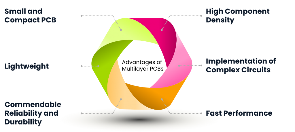
- Small and Compact PCB
The first advantage of multilayer PCBs is their compact size. These PCBs have a very small size, even if the design is complex. The reason behind this is the presence of multilayers. Thus, fewer circuits are on the board, and the components have more space. A multilayer PCB is perfect if you want a small PCB and PCBA. The assembly will take less space and make your final product compact. Due to this advantage and benefit, these PCBs are preferred over other types and are widely used in many applications.
- Lightweight
The final PCB is exceptionally lightweight compared to its single-layer and double-layer alternative. Due to the presence of multiple layers, there is no need for bulky jumpers and wires. All these are eliminated, and the complex design is implemented without wires. The interconnection of the layers also makes the circuit compact; thus, it reduces the weight.
Usually, there are SMDs on the PCB, so they save a lot of space and make the PCB lightweight.
- Commendable Reliability and Durability
Multilayer PCBs are more reliable. There are no external wires or other connectors that can create issues in the future. Everything is tidy and clean. The internal connection of the layers is more reliable than the external connector, and it offers the best performance even in extreme conditions. The durability of such boards is also commendable. They can withstand more pressure and temperature stress. The board is thick due to the core, copper layers, and prepreg, so it is more durable than a single-layer PCB or double-layer PCB.
- High Component Density
Multilayer PCBs have a very high component density. They save space on the surface layer, which is why more components can be placed. Moreover, the SMDs are compact, requiring only a little space. The components can be placed on both sides of the PCB, ensuring more components in a small space.
- Implementation of Complex Circuits
Complex and complicated designs can be implemented on multilayer PCBs. They have more layers, so it can be easily implemented no matter how complex your design is. However, it requires expertise in design.
- Fast Performance
Jumpers and wires take more time to transmit the signal because there is a considerable distance between the sender and receiver. On the other hand, multiplayer PCBs do not use jumpers and wires. The distance between the layers is minimal; one layer is just beneath the other. Thus, the performance is commendable.
What are the Disadvantages of Multilayer PCBs?
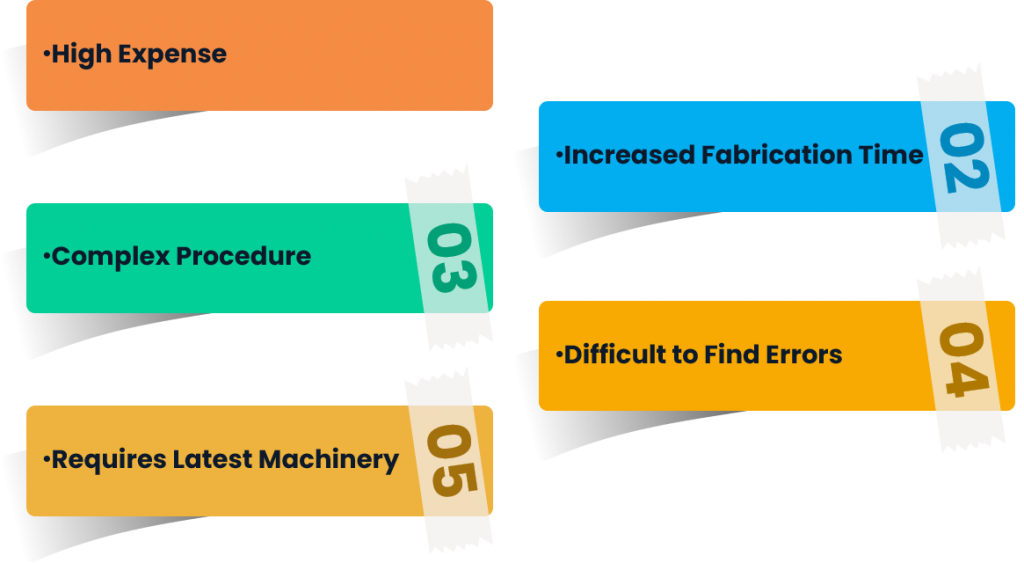
- High Expense
The cost of multilayer PCBs is much higher than other types. The reason behind this is the complex design that needs more expertise and exceptional requirements. The benefits come with an extra cost. However, people are willing to pay for a compact device and lightweight technology to get extra features. Therefore, multilayer PCBs are used in various applications, especially handheld devices, irrespective of the high price.
- Complex Procedure
The procedure of creating a multilayer PCB is quite complex. There are various layers, and the interconnection between them requires extra precision. The process is carried out by experts that understand the nitty-gritty.
- Requires Latest Machinery
The latest machinery is required to create multilayer PCBs; these cannot be created using the standard PCB machinery used for a single-layer PCB. Therefore, not every manufacturer can handle such PCBs.
- Increased Fabrication Time
Due to complex design and procedure, multilayer PCBs require more time. The buyer must wait, and the batch production is slow compared to single-layer and double-layer PCBs.
- Difficult to Find Errors
It is difficult to find the issues and errors in multilayer PCBs. Due to the presence of SMDs, an X-ray inspection is required. Moreover, it is difficult to repair such PCBs and rectify the errors.
Development Trend of Multilayer PCB
With the development of electronic components to “light, thin, short and small,” multilayer PCB will become the most influential and vital category in the printed circuit board industry and become the leading product. The structure of Multilayer PCB will be a diversified, thin, and high multilayer. At the same time, multilayer PCB also requires high equipment and technical investment.
- High density
- High multilayer
- Thinness
- Structural diversification
- High-performance thin copper foil and thin substrate
- The high flatness of plate surface and surface coating technology
- Flexible multilayer board and rigid-flexible multilayer board
Multilayer PCB Manufacturer in China
- Production of 1-32 layers of high-difficulty circuit boards, HDI, buried/blind vias, high frequency, High TG, Heavy Copper, Aluminum PCB, Flexible PCB, and Rigid-flex multilayer PCB and other circuit boards.
- FR4 Single-sided PCB,Double-sided PCB,Multilayer PCB Board,Single/Double-sided Aluminum PCB,Single/Double-sided FPC(Flexible Printed Circuit),High-frequency PCB, etc.
- Surface treatment process: HASL, Lead-free HASL, ENIG, Immersion Gold, Immersion Silver, Immersion Tin, OSP, etc.
- PCB Prototype, PCB clone; multi-layer PCB rapid prototype manufacturing, mass production, turnkey PCB assembly service, fast delivery within 24 hours.
Fast Delivery Service
- PCB Prototype Service: 1 day (24 hours expedited), two days for multi-layer PCB circuit boards (48 hours expedited), 4/6 layer PCB circuit boards: 3 days (72 hours expedited), eight layers PCB circuit boards; 4 days (96 hours expedited)
- Low-volume: 5-7 days, depending on the quantity, about eight days for multi-layer PCB circuit boards.
- Mass Production: 7-8 days, the multi-layer PCB circuit board 10-12 days.


