
BGA PCB - Ball Grid Array PCB Manufacturing and Assembly Service
Home » PCB Manufacturing » BGA PCB
Ball Grid Arrays - BGA Technology
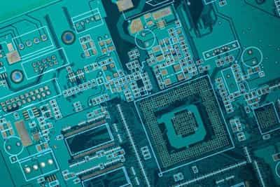
With the advancement in technology and the requirement of compact, reliable, and space-saving designs, there are different types of PCBs available, and BGA PCB is one of them. It is a special PCB used to accommodate BGA components. Nowadays, BGA components and chips are present in a wide range of products, so BGA PCBs have a high demand.
BGA PCB Fabrication and Assembly Supplier and Manufacturer
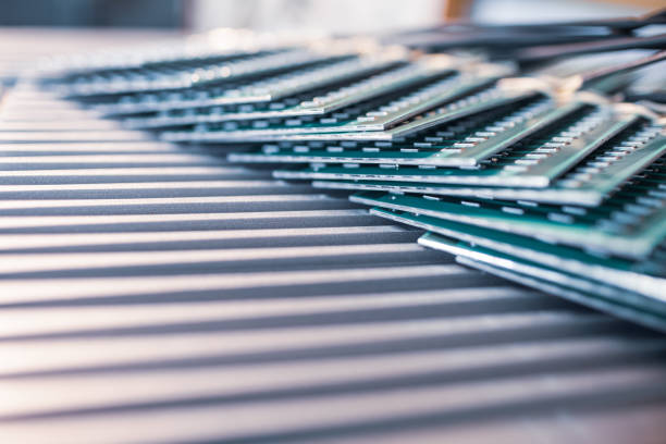
BGA PCBs are not like standard PCBs. They require the latest technology for manufacturing, assembling, and testing. JHYPCB, a professional and efficient PCB manufacturer in China, brings the perfect solution to all your BGA PCB needs. We are well-equipped with technology and can offer any complex or straightforward BGA PCB fabrication or assembly service.
BGA PCB Design Guide, Fabrication and Assembly Services
What does BGA stand for?
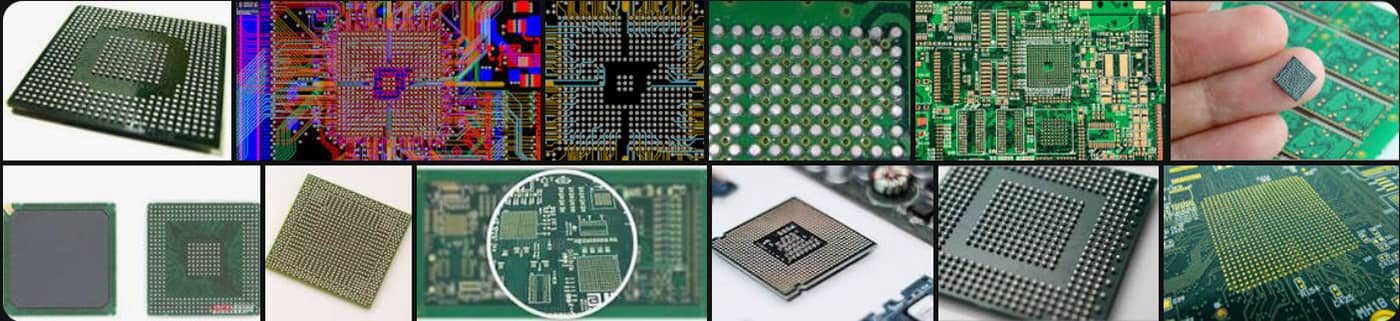
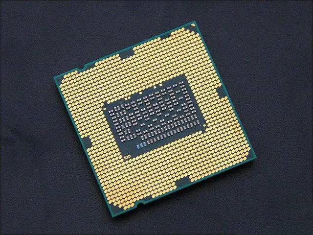
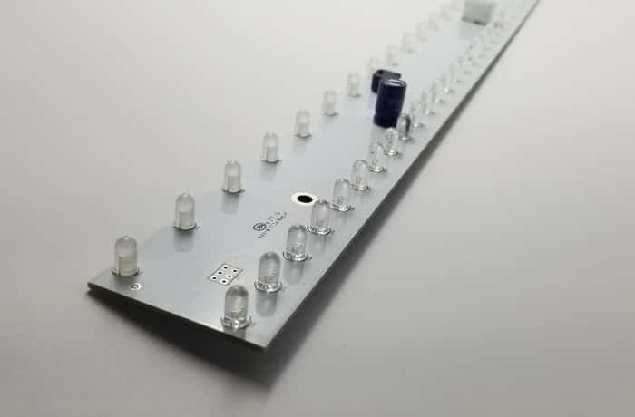
BGA stands for Ball Grid Array. The name explains everything but requires a bit of attention. BGA refers to an array of balls that are arranged in a grid or matrix fashion, just like the image on the right.

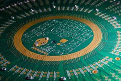
What is BGA PCB?
The PCB used for placing the BGA components is known as BGA PCB. It contains similar connections, just like the ball grid array present on the back of the BGA package. The component is placed over the PCB and then soldered. After soldering, the package looks as if it is pasted on the board with glue. There are no leads or connections on the side of the BGA package, and it makes the PCB more reliable and offers many benefits.
What is The Role of BGA in PCB Assembly?
The same ball grid array is created under the BGA package (component) and over the BGA PCB. These balls provide the connection of the component with the PCB board. The balls are made from the soldering material so that they can connect with the board.
The BGA component is a special type of surface mount component. These components are also mounted on the surface of the PCB without the requirement of holes. However, their connection with the board is not visible as the balls are present under the component.
BGA components look clean on the PCB board as their connections are hidden, and they offer dozens of advantages over Quad Flat Pack (QFP) components. Due to the constraints of the other types of SMD, BGA components are preferred for better performance in places where other SMDs cannot work or are unreliable.
Advantages of BGA PCB and Package:
There are many advantages of using BGA PCBs over other types of SMDs. It actually solves many constraints and problems of QFP and other SMD types. Due to the exceptional advantages, BGA is preferred in modern devices.
The first advantage of BGA is that it has more leads. If we look at the QFP package, we will find out the leads are present on the sides of the components. Therefore, there is not much space available, and only a few leads can be placed at a suitable distance. On the other hand, in BGA, the connections are present at the bottom of the component, so there is a lot of space available to accommodate more leads. Thus, BGA is the preferred option when it comes to the requirement of more leads.
There is a lot of space present under the component. So, the leads are placed over a suitable distance. They are not tightly packed, just like in the QFPs. This ensures the mitigation of short circuits between the leads. Therefore, BGAs are more reliable, and there are fewer chances of errors and issues in the future.
BGAs also save space on the PCB. The connections are made under the package, so there is no space required around the sides of the PCB. In the case of QFPs, the leads are on the sides; therefore, there should be some space for the connection. In simple words, BGAs use the space of the board wisely.
BGA components/packages are thin and compact. It is because they do not have pins coming out from the sides. Thus, the resultant BGA PCB is also compact. This is why it is preferred in mobile phones and other compact devices.
The electrical performance of BGAs is also better. The space or distance between the package and BGA PCB is minimum, which results in low resistance and low inductance. Therefore, it offers better conduction and transmits the signal in less time.
Components need to dissipate the heat; otherwise, there could be a component failure or any other issue. In BGAs, the heat produced by the components is directly transferred through the balls. Moreover, the contact area is large, which improves heat dissipation. This proves BGA has low thermal resistance, and the heat can be dissipated easily. It prevents the overheating of the components and ensures long life.
BGA components are tightly packed to the boards. They are robust and durable. Even under high vibration, these components stay at their place and offer excellent performance even in extreme conditions.
Disadvantages of BGA PCB:
Some disadvantages of BGA are:
- The solder balls are not that mechanically compliant. This means that mechanical stress can cause the joints of solder to fracture or break.
- The inspection of the faults is a bit difficult. Ordinary techniques, such as AOI, are not possible as BGA the connection is under the components.
BGA PCB Fabrication and Assembly Supplier
Types of BGA - How Many Types of BGA Are There?
BGA can be classified into the following types based on different substrates used:
1) PBGA (Plastic Ball Grid Array)
PBGA stands for Plastic Ball Grid Array. The BT resin is used as the substrate material. The solder balls used in this type are made up of tin and eutectic lead. This type of BGA is also capable of being used in flip-chip designs, which are helpful in increasing the connectivity between the circuit board and the package.
PBGAs are double-sided PCBs that can have almost 500 ball arrays; therefore, they can be used for multiple applications simultaneously. Also, there is no such need for any extra soldering between the package and solder ball. It also has additional copper layers to assist thermal dissipation.
The performance of PBGAs is very high in terms of electrical conduction. Moreover, they have higher thermal compatibility with PCB boards. The cost of PBGA is also low as compared to other types of BGA PCB. It also provides ease of surface mounting.
2) CBGA (Ceramic Ball Grid Array)
CBGA stands for Ceramic Ball Grid Array, and ceramic is used as the substrate here. In its design, there is a metal cover to protect the components that are being soldered onto the base. This increases the strength of the overall design.
If we calculate the cost per pin, then CBGA PCBs are expensive compared to PBGA. However, there are some applications where CBGA is preferred due to high pin count, as PBGA cannot be used due to its low density in this matter. For instance, in the automotive sector, high reliability is required no matter what the cost is; therefore, CBGA is used.
The solder balls in CBGA have a very high Lead percent compared to tin (90:10); this composition makes way for increased reliability and counters the problem that arises due to different thermal coefficients of substrate and board. CBGAs have high reliability due to better airtightness, and insulation is also better than PBGA.
3) TBGA (Tape Ball Grid Array):
Tape BGA is suitable for applications where high efficiency is required along with thin packaging and no additional heat sink. The chips can be placed up or down, but if they are placed up, the wire bond is optimum, while the flip-chip approach is recommended for chips to be placed down. Of course, the cost is also high for such a design.
In TBGA, the surface tension between solder balls could be adjusted to meet the alignment needs of solder balls and pads, and the tape provides better thermal compatibility to PCB boards. The only few problems with TBGA are its sensitivity to humidity and low reliability.
4) EBGA (Enhanced Ball Grid Array)
EBGA is an enhanced type of PBGA where the only difference between PBGA and EBGA is the additional heat sink. In this type, the chips or electronic components are sealed by a liquid compound, and they are always faced down. The connection between PCB and chip is achieved through a wire bond. It has a very high heat dissipation ability and very thick copper plates that remove heat from the die to the customer board.
5) FCBGA (Flip Chip Ball Grid Array)
FCBGA is similar to CBGA, but instead of Ceramic, BT resin is used as a substrate. Due to the presence of BT resin, it is cost-effective. Also, better electrical performance is achieved by reducing the pathways. The tin and lead ratio are 63:37, and this type of material can be adjusted for correction without any need for a flip-chip alignment machine.
6) MicroBGA
MicroBGA consists of chips that are faced down, and the packaging tape is used as the substrate. In this type, elastomer, a polymer with viscoelasticity, is used to release the stress created due to thermal expansion.
MicroBGA is very light in weight and can be used in places that have space-related constraints and where a low number of pins are required. It is smaller than the standard BGA. The three types that are commonly used in the industry are 0.65, 0.75, and 0.8 mm.
BGA PCB Applications
BGA packaging technology has been applied since the 1990s, and is now mainly used in high-end equipment, with huge room for development.
- Military applications
- Consumer Electronics
- Automotive Sector
- Flat Electronics Systems
- Integrated Circuits in TVs, computers, smartphones, etc.
BGA PCB Design Guidelines
How to Successfully Design With a BGA
While talking about BGAs, the pitch is an important factor, whether BGA PCBs or packages. While choosing a component or PCB, the pitch needs to be considered. It is mentioned in the component datasheet, and while designing the PCB, the pitch should be according to the component. Pitch is the distance between the centers of the adjacent balls. The commonly available pitches are 0.40, 0.50, 0.80, 1.00, and 1.27mm.
BGA PCB Layout
In starting a PCB layout with a BGA, there are a few tasks required to ensure successful routing:
- Signal layer count: Determining the number of signal layers needed in the stackup will influence the number of plane layers, as well the resulting trace width needed to route into the design.
- Fanout: How will signals enter and exit the BGA? Is controlled impedance needed? These questions will determine the layer count in the stackup, which will then determine how traces will be routed in the inner layers.
PCB layout with a BGA in three Strategis
- BGA Strategy 1: Defining Suitable Exit Routes
- BGA Design Strategy 2: Ground and Power
- BGA Design Strategy 3: Determining the PCB Layer Stack
How to Successfully Design With a BGA? Here is a very detailed BGA design proposal for reference.
Full-Feature BGA PCB Assembly Services
Soldering, Desoldering, and Reballing of BGA
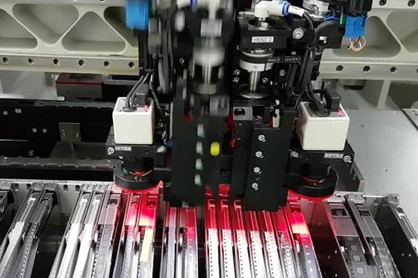
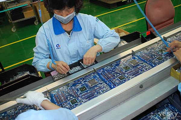
Our BGA PCB service cover a wide range, including BGA prototype PCB fabrication, BGA PCB assembly, BGA component removal, BGA replacement, BGA rework and reballing, BGA PCB assembly testing and inspection, and so on. Leveraging our full-feature BGA services, we can help customers streamline the supply network and accelerate product development time.
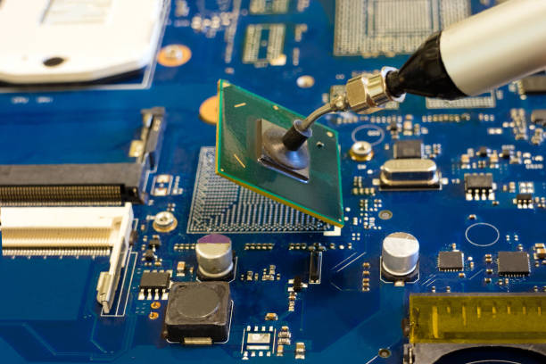
How to solder BGA to PCB?
The connection or pads are present under the package, which is why traditional soldering methods cannot be used. In QFPs, the leads are visible, and they can be easily soldered, but in BGAs, the leads or pads are not visible; they are hidden under the package. Thus, the only method that can be used is by melting the balls or solder to make the connections with the PCB.
Reflow methods are used for the soldering of BGA components. In this method, the components are placed over the PCB, and the assembly is heated. This melts the solder present under the component and joins the component with the PCB.
A reflow oven is used in the process for soldering the components; therefore, the most important thing is temperature control. Everything depends on the temperature. If the temperature is too high, the solder will melt and create a short circuit between the pads. If the temperature is too low, the solder will not melt properly; the component will not create a perfect electrical connection. Thus, the temperature and time must be monitored to prevent any problem in the soldering.
How to remove the BGA from the PCB?
After the completion of the BGA assembly, the assembly goes through an inspection. If there is any problem found in the connection of the component, it is desoldered. The desoldering is done by applying heat at the rework station. It melts the solder under the component, and then the component can be easily desoldered. The remaining solder left on the board is then cleaned.
The rework station has every tool. It can desolder the components and clean the PCB area. After desoldering, a new package could be used. However, the old component can also be used if it has no issue. The solder from the old component is removed, and reballing is done. Reballing refers to making a new balls grid array at the bottom of the component. Finally, the component is placed over the BGA PCB and soldered again.
Reworking must be done on a rework station because it offers more precision and control. The components can be aligned using optical alignment, and the required temperature is applied to ensure a perfect connection between the components and the PCB.
How are BGA Joints Inspected?
The Methods of Testing and Inspection the BGA Assembly Board.
BGA solder joint inspection cannot be carried out through traditional inspection methods. In optical techniques, such as AOI, cameras are placed at different angles. The cameras take images of the component and compare the results with the files. Workers can also see the images on a computer. Unfortunately, the cameras can only inspect the upper surface; they cannot take the image of connections under the component. Thus, the optical techniques cannot be used in BGA because the joints are hidden underneath the components.
The only test that could be accurately applied in this case and can provide optimal results is BGA inspection through X-Rays. The rays can be passed through the component and create a complete image of the connections underneath the element. If there is an issue, it is detected. X-ray inspection is an advanced technique, and with the help of this, it is possible to look under the device and examine the joints. Due to these features, X-ray inspection has become the leading technology for checking BGA PCB assemblies.
Advanced learning
Important Things to Consider in BGA PCB Assembly
- Positioning of the Component: The solder pads/balls under the component are quite small. They must be placed accurately on the board. The components are quite small; therefore, there are more chances of misalignment. It is necessary to place the component properly and then pass it through the reflow oven.
- Soldering Temperature: Soldering temperature plays an important role in the performance of the PCB. If the components are correctly soldered to the board without any open and short circuits, the PCB will provide the expected results. The temperature and time of the reflow oven must be controlled precisely to ensure the proper connection of the components with the board.
- Solder Paste Volume: Solder paste is applied to the BGA PCB before the placement of the components. For all SMDs, solder paste volume is important. If the solder paste is too much, there are chances of short circuits, and if the solder paste is too low, the component will not be connected properly. Thus, the volume of the solder paste is important. In the case of BGAs, the volume is more important than other SMDs as the paste is under the component and creates issues if not applied properly. For proper application of solder paste, a stencil is used. The volume of the solder paste depends on its stencil; if the stencil is correctly made, the solder paste will be applied as required.
- BGA Component and PCB Pad Size: The size of the pad of the BGA PCB should match with the ball grid array under the component. This has the utmost importance as the connection depends on it. Special care must be taken to ensure proper pad sizes in the BGA PCB according to the component.
BGA PCB Assembly Capability
Our BGA PCB assembly has automated placement systems. And they have Vision Systems that help to examine solder ball coverage.
An automated system with a 3D laser is also available. It helps to inspect the automatic placement of the solder ball height of MBGA, CBGA, and PBGA. Plus, we confirm our BGA assemblies with a real-time X-ray system.
You can place your orders with a minimum size of 0.3mm. The minimum space between two BGA is 0.2mm. And the minimum distance to the circuit line is 0.2mm.
What if your specifications are higher?
Don’t worry. All you need to do is state your specific requirements and leave the rest to us.

Get Your BGA PCB from JHYPCB
JHYPCB is a leading manufacturer of PCBs and PCBAs. We have a large facility in China, having more than 500 employees and experts. We can easily handle low-high volume orders. Our facility is equipped with the latest technology. We offer BGA PCBs and all services from manufacturing to testing. You can order even one PCB for your project.
JHYPCB is ISO, UL, and RoHS compliant. We have a strict quality management system that ensures high-quality PCBs on time. You can get the solution to all your PCB problems under one roof. We provide prototype PCB, batch production, and quick PCB assembly services. Your PCB or PCBA will be delivered without any hassle.
Contact us anytime for more information and details, and our customer support team will answer your queries and questions.
BGA PCB Design Guide, Assembly and Soldering Videos
How to fanout a BGA – Altium Designer 16.1
BGA Soldering
Ball Grid Array Rework: Package on Package Devices
How to inspect BGA Soldering performance on PCB
Recommended PCB Manufacturing Services
Related PCB Assembly Services
Helpful Resources
- JHYPCB Manufacturing Capabilities Introduction
- JHYPCB Factory Introduction
- How to Choose the Right PCB Manufacturer and Supplier
- PCB and PCBA Manufacturing Files
- The most comprehensive Introduction of Solder Resist for PCB
- What is the difference between SMT and SMD?
- What is the difference between wave soldering and reflow soldering?