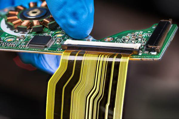
Gold Fingers PCB Circuit Board
Here’s everything you need to know about the Goldfinger circuit board
Home » PCB Manufacturing » Gold Finger PCB
Everything you want to know about Gold fingers PCB
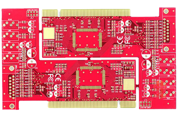
6 Layer Gold Fingers PCB
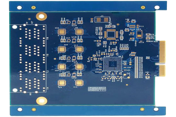
Double Layer Gold Fingers PCB
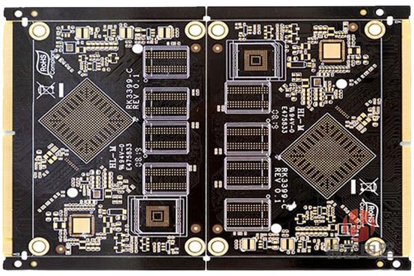
Double-sided Gold Fingers PCB
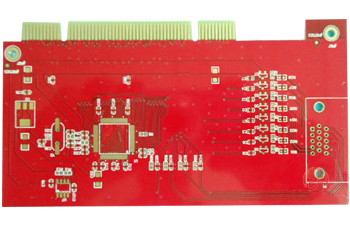
Double Layer Gold Fingers PCB
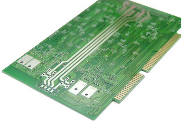
Gold Fingers Circuit Board
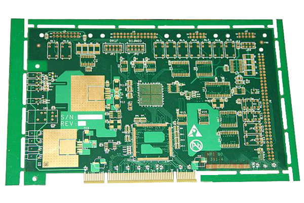
Gold Fingers PCB Board
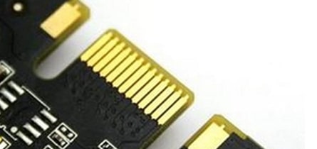
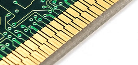
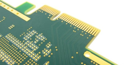
What is a Gold Finger PCB?
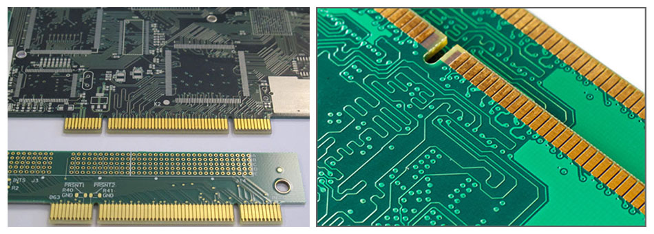
You might have seen PCBs with golden connectors. It is quite common in memory cards, graphics cards, hard drives, RAM, mobile phone components, and hundreds of other places. These gold fingers are the connectors that help you create an electrical connection of the Gold Finger PCB with another PCB.
The connectors are gold plated, and they have a resemblance with fingers; thus, they are named gold fingers, and the PCB is called Gold Finger PCB.
The connectors are located at the edge of the PCB and ensure the proper connection. The technology eliminates the use of cable connectors as the PCB can be directly connected. It is a more reliable, durable, and efficient option.
You might have noticed the distance between the fingers. This is to ensure the separation of connections from one another. The number of connectors, spacing, thickness, chemical composition, and other things are considered while designing the PCB.
Because of these gold connectors, you can connect the PCB without any hassle and as many times as you like. It makes connection, removal, and reconnection possible and straightforward. It is less prone to damage and wear and tear.
Why is Gold Finger PCB Used?
The main purpose of creating gold fingers along the edges of the PCB is to create a reliable and long-lasting connection with the other PCB. The gold fingers are a source of connection, and they are connected with a larger or the main PCB.
Sometimes it is necessary to separate different functions in different PCBs. For instance, the motherboard of the computer is the main PCB, but RAM is another PCB that works as temporary memory. It remains separated from the main PCB so that you can take it out and reinstall it or replace it without any hassle.
Gold fingers also help in accommodating extra components or devices. For instance, there can be multiple RAM cards in a computer. So, it is up to the user whether he wants to use an extra one or not. The same is the case with memory cards. The external memory card is not necessary, but you can increase the storage whenever you want.
Gold fingers provide a reliable means of connection between the two PCBs, devices, peripherals, adapters, and external connectors. They connect the PCB with the main PCB or power source. They help in transmitting the signals from one PCB to another without the need for cable connectors.
Surface Treatment of Gold Finger PCB
- Nickel gold plating: the thickness can be up to 3-50u “. Due to its superior conductivity, oxidation resistance, and wear resistance, it is widely used in the gold finger PCB, which needs to be plugged in and out frequently or the PCB, which needs to be subject to mechanical friction. However, because of the high cost of gold plating, it is only used in the local gold plating treatment, such as a gold finger.
- Immersion Gold: the thickness is 1U in general and 3U in maximum. its excellent conductivity, flatness, and solderability are widely used in high-precision PCB boards designed by key position, binding IC, BGA, etc. For the gold finger PCB with low wear resistance requirements, the whole board immersion gold process can also be selected, and the cost of the immersion gold process is much lower than that of the electronic gold process. The color of the immersion gold process is golden yellow.
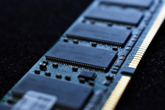
Why is Gold Used for Plating?
There are various metals out there, but why is Gold used to make the fingers? Can’t it be Silver Fingers or Copper Fingers?
These questions confuse beginners and people who don’t know much about PCBs. It is true that there are many metals available; however, not every metal can provide the performance that Gold provides.
Copper is the best conductor of electricity as it offers the best conductivity, 29×105 Ω-1cm-1. It means that copper can provide better conductivity than gold, but it cannot resist oxidation and corrosion. Thus, it is not used to make gold fingers. The same is the case with Silver. It is also a better conductor than gold, but it cannot survive for a long time. It can react with chloride and sulfide compounds/molecules in the air.
You might have also seen that the conductive layer of a circuit is made of copper, but it is protected by a surface finish of gold or any other protective material. It is because copper can undergo oxidation, which will create a hindrance in conduction.
Gold offers the utmost resistance against oxidation and environmental effects. It does not react with the particles in the environment and shows an inert behavior. This inertness makes it the best metal for making gold fingers.
Gold is also an excellent conductor after Copper and Silver. It offers 0.36×10⁵ Ω-1cm-1 (conductivity). Thus, its inertness and conductivity are the reasons behind its use to make gold fingers.
It is necessary to harden gold before applying it to gold fingers. The metal itself is not as rigid as required. So, it is mixed with Cobalt to make the metal stronger and rigid. About 5-10% of Cobalt is used to improve the properties of gold. The alternative for Cobalt is Nickel, and it can also be used.
After mixing gold with these metals, it can survive for a long time. We know that gold finger PCBs are frequently taken out and reinstalled. But the hardness of the alloy makes them super strong, durable, and reliable.
| Contact Material | Resistivity (Ωcm) | Contact Resistance (mΩ) |
|---|---|---|
| Pure Gold | 2.4 X 10⁻⁸ | 0.8 |
| An alloy of Gold and Cobalt | 2.4 X 10⁻⁸ | 2.6 – 2.8 |
| Palladium on Nickel | 1.08 X 10⁻⁷ | 3.1 – 5.8 |
| Silver | 1.6 X 10⁻⁸ | Non-determined |
Applications & Limitations of Gold Finger PCBs
The uses of PCB gold fingers can be divided into both technical (applications on circuits) and industrial/commercial applications. Let us begin with the Technical form of the contact fingers
Firstly. Technical Applications Of Gold Finger PCBs
Within the circuit, PCB gold fingers have several uses. Some of the technical applications of the connectors are:
They connect a PCB to a power source: one of the contact fingers’ primary uses is to connect a module PCB to a power source on a larger PCB’s connecting profile.
They help transfer signals/data: primarily, gold fingers link with the other PCBs to ease the data transmission and signals between the peripheral PCB and the giant board.
They interconnect modules within the same board: traditional electronics used to consist of several robust modules that could not be interconnected easily within the same board. With the aid of flexible PCBs, electrical engineers could interconnect multiple modules even within the same board.
They provide room for future improvements: well, imagine a computer motherboard without ports and expansion slots. How would it look like? How would it function? And would other interested electricians improve it without adding expansion slots or vendor modules? The picture is unimaginable. You would not be able to connect input devices and output devices. Other engineers would not have worked on improving a computer’s keyboard or mouse or VGA card. Simply put: without having gold finger PCBs, machines cannot be improved.
Secondly. Commercial applications
In the industry, gold fingers PCBs are used in several areas. Some of the popular applications include:
They are used to provide connections for data transfer on network-enabled devices. I.e., we apply Gold fingers in the manufacture of network cards and other additional networking PCB modules.
They are used to attach specialty adapters. Edge connectors provide an attachment area for special adapters like Video Graphic Array (VGA) cards and other video cards useful in processing images. These additional specialized modules relieve the mainboard of some of the processing that is useful when computing.
They are used to connect other devices to the central processing board. Besides the advantage of connecting network modules and specialized adapters, you can also use gold finger PCBs on the connecting edges of peripheral devices that get connected to the mainboards. Their application is relevant in producing devices like Memory card adapters/readers, flash-drives, among other methods. These additional devices can help in boosting processing, adding storage memory, or powering the mainboard.
They are also used to connect audio adapters to main PCBs.
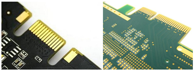
Important Things You Should Know About Gold Finger PCB
- There are various base materials for gold fingers PCBs. You can even have gold fingers on a flexible PCB.
- You will also find gold fingers of different sizes. The size of the gold fingers can be adjusted as required. Some can be shorter, while some can be longer. There can be segments in fingers as well.
- The edges of the gold fingers are beveled. It means they have a slope or pointed form. Beveling can be done at various angles as required. Typically, the angle ranges from 30°-45°. It ensures the easier and more proper connection of the PCB board.
- Gold fingers are expensive, but it is necessary to use gold in them. However, you can try ENIG (a type of surface finish) for prototypes. It will save you some money, but keep in mind that it is only suitable for prototypes as it won’t last for a long time. For final PCBs, you must select hard plated gold.
- There can’t be vias under or near gold fingers.
- You can plug in a gold finger PCB up to 1000 times. They can prevent wear and tear.
- The thickness of the gold plating can be according to the requirements. It depends on the expected attachment and detachment of the board. It is usually in the range of 3-50 microinches.
- Silkscreen and solder mask should be away from gold fingers.
How Gold Fingers Are Changing the World
Today’s computer and mobile devices are growing ever-more complex as manufacturers compete to make their products faster and more resourceful. If you build a massive computer station and amass a handful of mobile devices, you are liable to have numerous gold-plated circuit boards interacting at the same time. Each time you print out an article or scan a photo to upload to a social media account, signals are sent from peripheral devices to motherboard cards, which receive these signals via PCBs.
Thanks in large part to gold fingers, technology has been able to advance to the new array of mobile devices that millions now use daily. Moreover, gold fingers have allowed industries to become more productive and capable than ever before.
As increasing amounts of technology rely on gold fingers, it is crucial to have them plated and tested to the highest standards. Only this way can you ensure maximum performance without fail from the tech products that use circuit boards. At JingHongYi PCB (HK) Co., Limited, we provide PCBs of the highest quality for customers in various industries.
Get Gold Finger PCBs from JHYPCB
JHYPCB is a complete PCB and PCBA services provider and leading manufacturer in China. We can provide all types of PCBs and PCBA services at a very reasonable cost. Our large facility can handle low-high volume orders with the help of 500+ experienced employees.
We can provide you Gold Finger PCBs according to your requirements. We understand the industry standards and rules followed to create gold fingers. We take care of everything to ensure safe, reliable, and optimum performance. Our quality management system is quite strict and ensures high performance. We are certified by RoHS, ISO, and UL. Thus, customers can place their orders with confidence, and we will provide the best services according to international standards.
We can help in creating prototypes and complete assemblies. We offer quick turnaround and turnkey assembly services. Our buyers can even order one PCB to check their design. For more information and details, feel free to contact us.
Related PCB Fabrication Services
Related Posts
- Custom PCB Manufacturer In China
- Why Choose Chinese PCB Manufacturer
- Fast Turn Prototype PCB Service
- Basic Knowledge of PCB Pad Design
- 10 Tips To Improve PCB Design For Manufacturability
- PCB Design Software Free Download
- Find Out Now, What Should You Do For Fast PCB Classification?
- What Is FR-4 Material In PCB Fabrication?
