
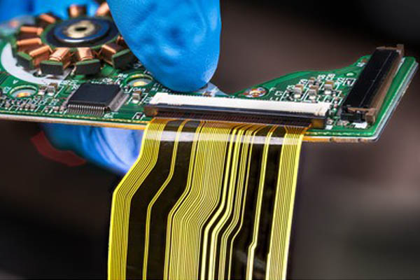
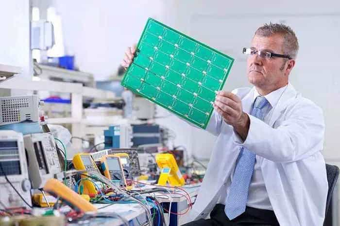
Testing & Inspection Methods for PCB and PCBA
Printed Circuit Board and PCB Assembly Testing: Competence, Acceptance, and Compliance
Table of Contents
What is PCB Testing?
PCB testing is the last quality control link in the PCB manufacturing process. Today’s PCBs are smaller and more sophisticated than ever before. With the increasing application of multi-layer PCB, the test method of PCB with a digital multimeter is not feasible. Fortunately, now we have more viable ways to test PCB. Any PCB manufacturer should do an excellent job in PCB testing and inspection before PCB leaves the factory.
What is the PCB test point?
PCB test points simplify and optimize the test process after PCB assembly. By setting test points at the PCB design stage, the subsequent PCB assembly test can be improved.
To improve production efficiency, we can’t rely on a digital multimeter to test whether each resistance, capacitance, inductance, and IC circuit on PCBA is unblocked, so we use the ICT test method.
However, ICT uses multiple probes (we call it Bed-of-Nails fixture) to contact all the circuits on the PCB board that need to be tested and detected simultaneously. If these probes directly contact the electronic components or their pins on the PCB, they will likely crush some electronic components. Therefore, intelligent PCB engineers create “test points.”
Design considerations for PCB test points
- The diameter of the test point is not less than 0.4mm, and the distance between adjacent test points is preferably 1.27-2.54mm or more;
- Components with a height of more than 6.4mm cannot be placed on the side of the PCB with test points;
- The distance between the test point and the edge of the PCB must be greater than 5mm;
- The test point cannot be covered by solder mask or silkscreen legend;
- The test point is best to be plated with solder or choose a soft, easily penetrated, and non-oxidized metal to ensure reliable grounding and prolong the service life of the probe;
- The test point should be placed 1mm away from the component to avoid collision between the probe and the component;
- The test point must be placed 3.2mm away from the positioning hole;
Why is PCB Testing and Inspection Necessary?
When it comes to electronic products, the printed circuit board (PCB) as the carrier of electronic components plays an important part. For any designer or builder to achieve ultimate success, it must perform PCB testing and inspection. Understanding and mastering the testing and inspection methods of printed circuit boards is essential to ensure that the products can work typically. By testing circuit boards, you can minimize significant problems, find smaller errors, save time, and reduce overall costs.
PCB testing and inspection are mainly used to find problems in the entire PCB manufacturing process and the final PCB assembly process. These tests can also be used on PCB prototypes fabrication or low-volume PCB assembly, which can help identify potential problems in the final product.
To ensure the PCB board’s final quality, PCB manufacturers use a variety of PCB testing and inspection methods during the PCB manufacturing and assembly process. Each detection method has its advantages and disadvantages and will target different PCB board defects.
We offer a wide variety of PCB testing and inspections for all boards we provide, both bare board fabrication and assembled PCBs.
PCB Test Features: IPC-6012, IPC-6013, IPC-6016, IPC-6018, MIL-PRF-55110, MIL-P-50884 or MIL-PRF-31032
Advanced learning: IPC Standards: A Guide to Standards for PCB Manufacturing and Assembly
The following are four important contents of PCB testing and inspection:
- PCB Function Test
- PCB Electrical Characteristic Test
- PCB Reliability Test
- PCB Mechanical (flexible) Test
1) The PCB Function Test
The function test is to use special test equipment in the middle and end of the production line to conduct a comprehensive test on the functional modules of the circuit board to confirm the quality of the circuit board.
PCB Function Test mainly includes:
- DFM Check
- Bare PCB Board Test
- ICT
DFM Check (Design for Manufacturing)
Bare board tests typically consist of the PCB manufacturer checking against netlists for “shorts” or “opens.”
Click here to learn”How To Testing A PCB For Short Circuit?“
The first step is the DFM test (Design for Manufacturing) with software that runs design rule checks against GERBER files.
DFM checks the design for shorts or opens, which can be very helpful before board fabrication even happens. But once the board has been fabricated, a simple bare board electrical test can save major problems from happening downstream.
Bare PCB Board Test
The bare PCB board electrical test is the electrical test when the SMT is not printed. It uses a multi-point testing machine to test the board. It mainly checks the circuit’s conductivity and determines whether there is an open circuit or a short circuit.
It finds manufacturing defects and tests analog, digital, and mixed-signal components through electrical performance testing to ensure that they meet specifications. There are several testing methods, such as bed-of-needle testers and flying probe testers. The main advantages are the low test cost of each board, strong digital and functional testing capabilities, fast and thorough short-circuit and open-circuit testing, programming firmware, high defect coverage, and easy programming. The main disadvantages are the need for testing fixtures, programming and debugging time, high cost of making fixtures, and difficulties in the procedure.
Testing Methods for Bare PCB Board
The bare PCB board test can be divided into the particular type, general type, flying probe, conductive adhesive and E-beam, capacitive and brush test. Currently, the most commonly used test methods are as follows:
Dedicated: It is only suitable for one material number. Boards of different material numbers cannot be tested and cannot be recycled. In terms of test density, due to the probe head’s thickness, it is more suitable for 0.02″ pitch boards.
Universal: Standard Grid fixes large needle plate with many measuring points can be made movable probe disc according to different material numbers. The movable needle disc is changed during mass production. Mass production testing of various material numbers can be performed.
Flying Probe Testing: Flying probe testing is a tried-and-true option that’s less expensive than in-circuit testing. It’s a non-powered type of test that checks for:
- Opens
- Shorts
- Resistance
- Capacitance
- Inductance
- Diode issues
The test works through needles attached to a probe on an XY-grid obtained from basic CAD. Your ECM program coordinates match the circuit board and then runs the program.
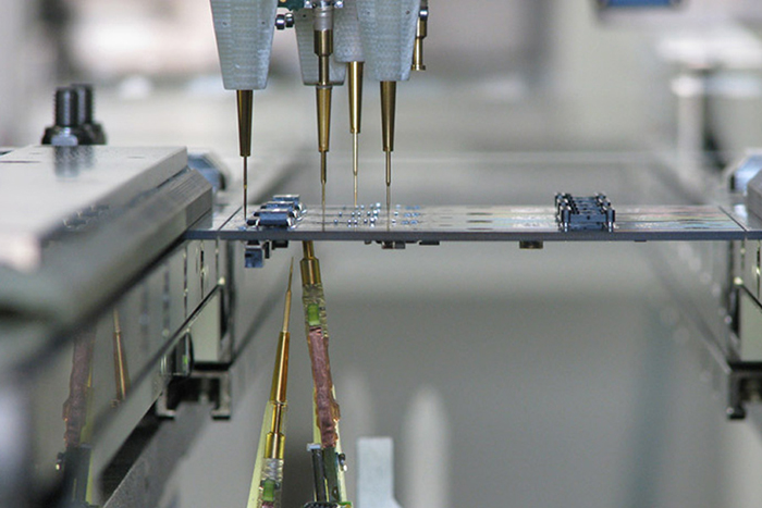
IN-CIRCUIT TEST
In-circuit testing (ICT) is the most robust type of PCB testing in existence. The high price reflects tens of thousands of dollars. However, the cost will depend on board and fixture size, among other factors.
The ICT, also known as a bed-of-nails test, powers up and actuates the board’s circuitry. In most cases, the test is designed for 100% coverage, but you’ll get closer to 85%-90% coverage. The nice thing about ICT is that 85%-90% you get is free of human error.
This test involves using fixed probes laid out in a way that matches the design of the PCB. The probes check the integrity of the solder connection. The bed of nails tester pushes the board down on the bed of probes to start the test. There are access points predesigned in the panel that allow the ICT testing probes to connect with the circuit. They put a certain amount of pressure on the connection to make sure it stays intact.
ICT is often performed on more significant connections and ball grid arrays (BGAs).
This test is for a “mature” product with very few revisions expected. If you don’t have design-for-manufacturing as part of your goal, with the proper pads on the board, you may not be able to use the in-circuit test. Unfortunately, you can’t change your mind and move to an ICT strategy halfway through production.
Flying Probe Test vs. ICT Testing
Let’s see Flying Probe vs. ICT. Each has advantages and disadvantages.
In some cases, ICT makes it unnecessary to use flying probe testing, but the PCB has to be designed to fit with the test fixture – which means a higher initial cost. ICT can be faster and less error-prone than flying probe testing, so you might find the extra cost is worth it. While flying probe testing can be cheaper initially, it may actually be less cost-effective for large orders.
One final word of caution: A PCB flying probe test does not power up the board.
2) PCB Electrical Characteristic Test
PCB electrical characteristics test includes the following:
- TDR Impedance Test
- Withstand Voltage Test
- Dielectric Insulation Resistance Testing
- Surface Insulation Resistance Testing
a) TDR Impedance Test
It tests the resistance encountered by high-frequency signals propagating in the PCB transmission line.
PCBs usually require impedance tests to ensure proper signal function. Impedance issues can cause performance and reliability problems that are easily detected through TDR (Time Domain Reflectometry) testing. The TDR test applies a very fast electrical step signal to the PCB or coupon through a controlled impedance cable and probe. Whenever there is a change in impedance value, part of the signal power is reflected back to the TDR tester. The data is recorded and saved by the TDR tester as well as graphed. The graph depicts the impedance values over the distance of the PCB or coupon under test. Data such as average, standard deviation, minimum and maximum values are also displayed.
Equipment for TDR Impedance Test: TDR-Time Domain Reflectometry
b) Withstand Voltage Test:
For reliability experiments, it tests the characteristics of the voltage that the medium between the circuit boards can withstand.
c) Interlayer (surface) Insulation Resistance:
It tests the PCB circuit and circuit insulation. It ensures there is conduction from the insulation, and it is working perfectly well. It checks the insulation between the conducting paths, contacts, and grounding devices.
3) Reliability Test
Purpose: To establish product reliability and test items and standards to ensure product quality.
Scope of Application: In-process and finished products of general PCB boards and HDI PCB boards, including independent inspection, manufacturing process testing, and testing of the items.
- Ion Pollution test: Tests the pollution degree of a printed circuit board
- Peel Test/Adhesion Test: Tests whether the strength of S/M, text, ink, and plating on the copper surface is qualified
- Solderability Test: Tests the board’s tin consumption to ensure the solder quality
- Hot Oil Test: Confirms the bonding and copper plating quality by immersing in a high-temperature oil tank.
- Tensile Test: Tests the adhesion between copper and PP
- Thermal Stress Test/Metallized Hole Thermal Stress Test: It tests the effect of thermal stress on the bonding quality and coating integrity of the finished board after baking and high-temperature impact. It observes whether the interconnection in the metalized hole is damaged and whether the glass cloth substrate has delamination.
- High Humidity Test: Detects the influence of high humidity on the quality of the product after the gold surface is subjected to high humidity
- Cold and Thermal Shock Test: Tests the quality of the coating and material structure of the printed circuit board under high and low-temperature cycle impact
- Solvent Resistance Test: Detects whether the finished board has abnormal phenomena, such as S/M dissolution and peeling after being soaked in the chemical solution
- Moisture and Insulation Resistance Test: Tests the influence of the finished board on its insulation resistance under high temperature and high humidity environment
- SMT Pad Heavy Industry Simulation Test: Tests the adhesion between the plating layer and copper and PP
- Through-hole repeated plug-in simulation test: the effect of multiple plug-ins on the quality and integrity of the hole wall of the part is simulated
- Dip Balance: Tests and use solder balance test pad and through-hole tin wetting ability
- SO2 Porosity Test: Tests the porosity of the gold surface after gold; if it is too large, it will cause poor corrosion resistance and affect product quality.
- Nickel Surface SEM/EDS Test: Detects the phosphorus content value and the crystallization condition of the nickel surface after the gold is treated
- Salt Spray Test: To verify the ability of FPC surface treatment to resist harsh environmental pollution and corrosion
- Dielectric Withstand Voltage Test: Tests the insulation performance of circuit board materials and whether the space between wires is sufficient
4) PCB Mechanical Characteristic Test
PCB mechanical characteristic test includes the flexural test and impact test.
7 Types of PCB Testing and Inspection Methods
1) PCB Section Analysis- The Most Important Analysis Method in the PCB Industry
PCB section analysis technology is one of the most common and essential analysis methods in the PCB industry. It is usually used for quality determination, quality anomaly analysis, an inspection of circuit board quality (checks the thickness of PCB internal traces, the number of layers, and the size of through-holes, through-hole quality observation, and interface bonding status), PCBA soldering quality inspection, finding the cause and solution of failure, evaluating process improvement (as a basis for objective inspection), research, and judgment.
PCB section analysis is an essential technique for PCB/PCBA failure analysis, and the quality of the section will directly affect the accuracy of the identification of the failure location.
The quality or appearance of the outer layer can be judged by optical inspection or visual inspection. Still, the quality of the laminated board’s inner layer or hole cannot be evaluated by testing or visual inspection. So, for the inner layer after the lamination or to confirm the quality of the hole, it is necessary to perform quality judgment through sections and make a preliminary analysis of the defect’s cause. PCB section analysis is an essential technique for PCB/PCBA failure analysis, and the quality of the section will directly affect the accuracy of the identification of the failure location.
PCB Section Classification:
General PCB sections can be divided into vertical sections and horizontal sections.
Vertical Section: Vertical section is cut along the direction perpendicular to the board surface to observe the cross-sectional condition. It is usually used to observe the quality of the hole after copper plating, the laminated structure, and the internal bonding surface condition. A vertical slice is the most commonly used method in slice analysis.
Horizontal Section: Horizontal section is ground down layer by layer along the stacking direction of the board. It is used to observe each layer’s condition, usually used to assist the vertical section in analyzing and determining abnormal quality, such as internal Short or abnormal inward opening, etc.
Oblique Section: The multi-layer PCB board is filled with glue through holes. The vertical direction is 45° or 30° diagonal section and oblique grinding. It is used to observe the variation of each layer of conductor lines on the tilted plane with a reliable microscope or high-power tomography microscope. In this way, the dual characteristics of straight cut and cross-cut can be taken into account. However, it is not easy to place it in a horizontal position for microscopic observation.
The Production Steps of PCB Section:
- Sampling
- Resin Encapsulation
- Grinding
- Polishing
- Microetching
- Photography
After the section is made, the section’s microscopic details are analyzed through a metallographic microscope and scanning electron microscope. Only when the section is correctly interpreted can the correct analysis be made, and practical solutions can be given. Therefore, the quality of the sections is particularly important. Poor quality sections can cause serious misleading and misjudgment of failure analysis. As the most important analysis equipment, the metallurgical microscope has a magnification ranging from 50 to 1000 times, and the measurement accuracy deviation is within 1 μm.
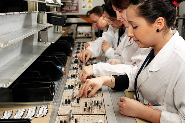
2) Manual Visual Inspection
After using a magnifying glass or a calibrated microscope, the operator’s visual inspection determines whether the circuit board is in compliance and when a correction operation is required. It is the most traditional detection method. Its main advantages are low upfront cost and no test fixture. In contrast, its main disadvantages are human subjective error, high long-term cost, discontinuous defect detection, and difficulty in data collection. At present, due to the increase in PCB production, the shrinking of the wire spacing, and component volume on the PCB, this method has become increasingly infeasible.
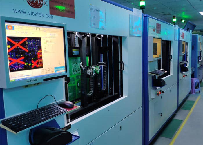
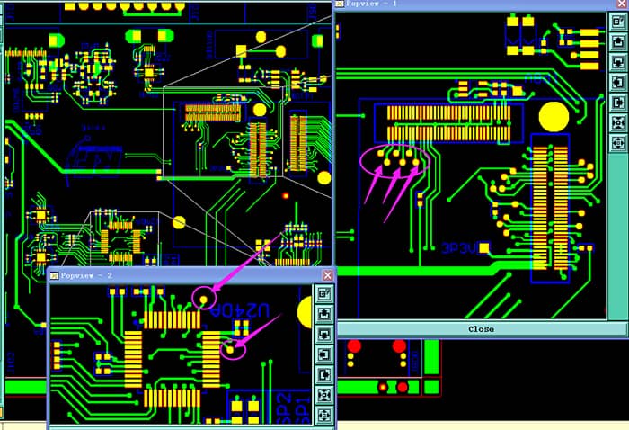
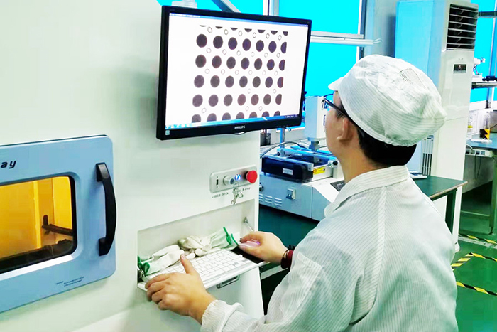
3) AOI
AOI stands for Automatic Visual Inspection. It is based on optical principles, combined with image analysis, computer and automatic control, and other technologies to detect and deal with defects encountered in production. It is a new method of confirming manufacturing defects. AOI is usually used before and after reflow soldering and before electrical testing to improve the pass rate of electrical processing or functional testing. At this time, the cost of correcting defects is much lower than the cost after final testing, often reaching more than ten times.
AOI uses either a single 2D camera or two 3D cameras to take photos of the PCB. The program then compares the photos of your board to a detailed schematic. If a board does not match the schematic to a certain degree, the board is flagged for inspection by a technician.
AOI can be useful for detecting issues early to ensure production is shut down as soon as possible. However, it does not power up the board and may not have 100% coverage for different components and parts.
Never rely solely on an automated optical inspection. AOI should be used in conjunction with another test. Some of our favorite combos are:
- AOI and Flying Probe
- AOI and In-circuit Test (ICT)
- AOI and Functional Testing
It is also referred to as AXI. This type of testing is really more of an inspection tool, at least for most ECMs.
During this test, an X-ray technician can locate defects early during the manufacturing process by viewing:
- Solder connections
- Internal traces
- Barrels
There are 2D and 3D AXI tests, with 3D offering a faster testing period.
Due to the difference in the absorption rate of different substances to X-rays, this method is used to see through the parts that need to be tested and find defects. It is mainly used to detect defects in ultra-fine pitch and ultra-high-density circuit boards and bridges, missing chips, poor alignment, and other defects generated during the assembly process. It can also use its tomographic imaging technology to detect internal flaws in IC chips. It is the only way to test the ball grid array’s soldering quality and the blocked solder balls. The main advantage is the ability to detect BGA welding quality and embedded components without fixture cost. The main disadvantages are slow speed, high failure rate, difficulty seeing rework solder joints, high cost, and extended program development time. This is a relatively new test. Therefore, the method remains to be further studied.
5) Laser Inspection
It is the latest development of PCB testing technology. It scans the printed board with a laser beam, collects all measurement data, and compares the actual measurement value with the preset qualified limit value. This technology has been proven on the bare board and is being considered for assembly board testing. The speed is sufficient for mass production lines. Fast output, no fixtures, and visual non-covered access are its main advantages. High initial cost, maintenance, and use problems are its main disadvantages.
6) Quadratic Element Dimensional Measurement
It uses the two-dimensional image measuring instrument to measure the hole position, length and width, position, and other dimensions. Because PCB is a small, thin and soft type of product, contact measurement can easily deform and cause inaccurate measurement.
The two-dimensional image measuring instrument has become the best high-precision size measuring device. The programmed two-dimensional image measuring instrument can realize fully automatic measurement, which has high measurement accuracy and dramatically shortens the measurement time and improves the measurement efficiency.
7) Hi-Potential Testing (Hi-Pot PCB Testing)
Hi-Pot testing is the opposite of a continuity test. The testing system injects high voltage signals and verifies isolation between areas on the PCB, ensuring that no current flows from one place to another.
This test is strongly recommended for high voltage circuit boards. Thin dielectrics sometimes go through Hi-Pot PCB testing as well.
In summary of the seven testing and inspection methods, optical inspection and X-ray inspection are still the most popular on the market.
Recommended PCB Fabrication Services
What is PCBA Test?
The process flow of PCBA processing is very complicated, including many essential processes, such as PCB board manufacturing process, component procurement and inspection, SMT patch assembly, DIP plug-in, and PCBA test. Among them, PCBA testing is the most critical quality control link in the entire PCBA process. It is an essential means to control product quality and determines the final performance of the product.
The functional test after the circuit board is assembled is generally called FVT (Function Verification Test) or FCT (Function Test).
What is the PCBA Test Principle?
Connect the test points on the PCBA board through the FCT test frame to form a complete path, connect the computer and the burner, and upload the MCU program. The MCU program will capture the user’s input actions (such as long-pressing the switch for 3 seconds), and control the on and off of the circuit beside it (such as LED flashing) or drive the motor to rotate through calculations. By observing the voltage and current values between the test points on the FCT test frame and verifying whether these input and output actions are consistent with the design, the test of the entire PCBA board is completed.
PCBA testing mainly includes five forms: ICT test, FCT test, aging test, fatigue test, and test under harsh environment.
- ICT test mainly includes circuit on-off, voltage and current value, fluctuation curve, amplitude, noise, etc.
- FCT test requires IC program firing, simulation test of the entire PCBA board function, and the discovery of hardware and software problems. It is equipped with the necessary patch processing production fixtures to test racks.
- The fatigue test is mainly to sample the PCBA board and perform a high-frequency and long-term operation of the function to observe whether there is a failure. It determines the probability of failure in the test to feedback the working performance of the PCBA board in the electronic product.
- The test in a harsh environment mainly exposes the PCBA board to extreme temperature, humidity, drop, splashing, and vibration. It obtains the test results of random samples, thereby inferring the entire PCBA board batch product’s reliability.
- The aging test is mainly to energize the PCBA board and electronic products for a long time and keep them working and observe any failures. After the aging test, the electronic products can be sold in batches.
What are the functional test methods of PCBA?
General part:
- Power Supply Test: It checks whether the power supply is working properly and tests each point’s voltage.
- Port (interface) Test: It checks whether there is a short or open circuit that can cause abnormality.
- Integrated Circuit Module IC I/O: It reads and writes Function test-Flash&EEPROM&CPU&SDRAM&Logic IC etc.
- Special Function Test (different circuit board requirements are inconsistent)-such as infrared ray, need an external receiver.
Other PCB Assembly Testing Types Include:
- Solderability Test: Ensures surface sturdiness and increases chances of forming a reliable solder joint
- PCB Contamination Testing: Detects bulk ionics that can contaminate your board, causing corrosion and other issues
- Micro-sectioning Analysis: Investigates defects, opens, shorts, and other failures
- Time-domain Reflectometer (TDR): Finds failures in high-frequency boards
- Peel Test: Finds the measure of strength required to peel the laminate from the board
- Solder Float Test: Determines the level of thermal stress a PCB’s hole can resist
Advantages of Functional PCB Testing Include:
- Simulates the operating environment, minimizing customer cost
- May eliminate the need for expensive system tests
- Can check product functionality – anywhere from 50% to 100% of the product being shipped; you need to check and debug further
- Pairs well with other tests, such as ICT and flying probe
- Great for detecting incorrect component values, functional failures, and parametric failures
PCBA test depends on what test you are doing, ICT, or FCT. Different test methods charge differently because ICT equipment and tooling are relatively expensive. However, ICT can give good test results and bring great benefits to repairs.
The PCBA process is complicated. Various problems may occur during the production and processing due to improper equipment or operation, and there is no guarantee that the products produced are qualified. Therefore, PCBA testing is required to ensure that each product does not have quality problems.
10 Types of PCBA First Article Inspection and Testing Methods
1) Manual Visual Inspection
Manual testing directly relies on visual testing to confirm the placement of components on the PCB through visual and comparison. This technique is widely used. However, the large number and small components make this method increasingly unsuitable. Some functional defects are not easy to detect, and data is not easy to collect. Therefore, more professional testing methods are needed.
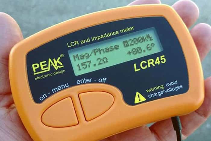
2) LCR Measurement
LCR measurement is suitable for some simple circuit boards. There are few components on the circuit board. There are no integrated circuits and only some passive components. After the placement is completed, there is no need to re-heat the circuit board. The device is measured and compared with the component rating on the BOM, and formal production can begin when there is no abnormality.
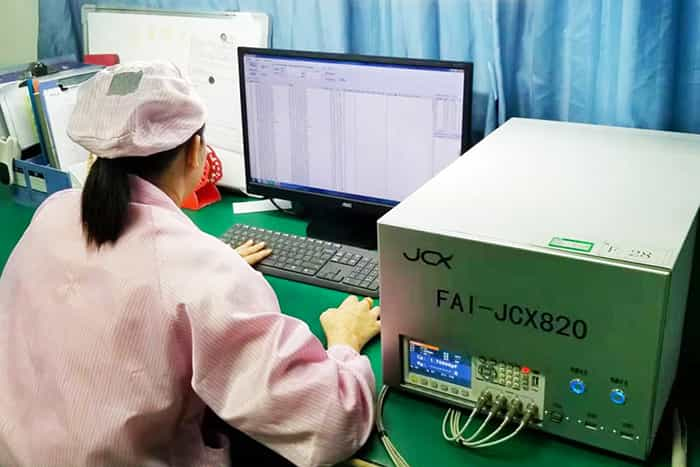
3) First Article Inspection (FAI)
The FAI first test system is usually composed of LCR bridges and integrated by FAI software. The product BOM and Gerber can be imported into the FAI system. Employees use their own fixtures to measure the first sample components, and the system will input them. The CAD data is checked, and the test process software displays the results through graphics or voice, which reduces the false test caused by the negligence of personnel search; it can save labor costs.
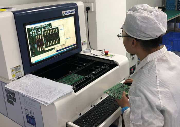
4) AOI - Automated Optical Inspection
This test method is very common in PCBA processing, applicable to all PCBA processing, mainly through the components’ appearance characteristics to determine the soldering problems of the component. You can also check the color of the components and the silkscreen on the IC to determine whether the circuit board’s components have the wrong parts.
5) X-RAY – Automated X-ray Inspection
For some circuit boards with hidden solder joints, such as BGA, CSP, and QFN packaged components, X-ray inspection is required for the first product produced. X-ray has strong penetrability. It is one of the earliest instruments used in various inspection occasions. X-ray perspective images can show the thickness, shape, and quality of solder joints and solder density. These specific indicators can fully reflect the welding quality of the solder joints, including open circuits, short circuits, holes, internal bubbles, and insufficient tin, and can be quantitatively analyzed.
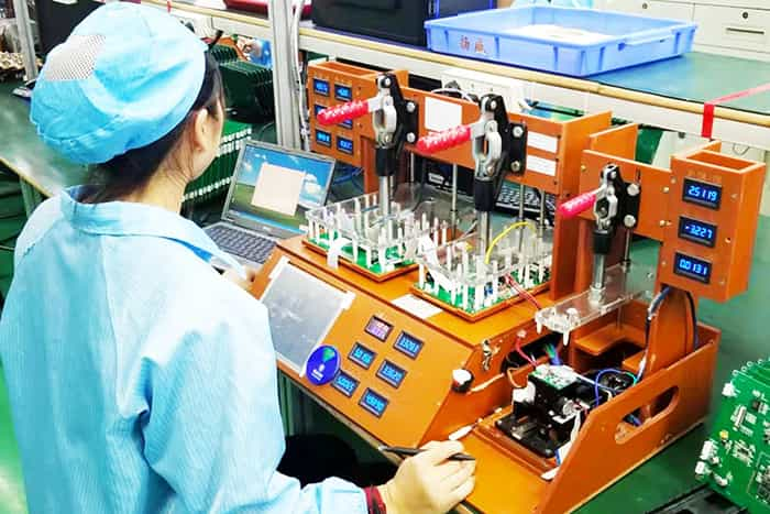
6) What is Flying Probe Test?
Flying probe test is usually used in some developmental prototype PCBA manufacturing and small batch production. It is characterized by convenient testing, substantial program variability, and good versatility. It can basically test all types of circuit boards. However, the test efficiency is relatively low, and the test time for each panel will be very long. It mainly measures the resistance between two fixed points to determine whether the circuit board’s total components have short circuits, without soldering, and wrong parts.
Now, the requirement of a test system with fast turning and no fixture capabilities required for prototype manufacturing and small-batch manufacturing makes flying probe testing the best choice.
7) ICT-IN Circuit Test
The in-circuit test is test equipment that is necessary for modern electronics companies. It has a wide range of ICT applications, high measurement accuracy, and an indication of detected problems. Even workers with average electronic skills can handle problematic PCBAs easily. The use of ICT can significantly improve production efficiency and reduce production costs.
ICT Test mainly tests the PCBA circuit open circuit, short circuit, and welding condition of all parts by connecting the test point of the test probe to the PCB layout. It can be divided into open circuit test, short circuit test, resistance test, capacitance test, diode test, triode test, field-effect tube test, IC pin test (test jet connect check), and other general and special components, such as missing installation, incorrect installation, parameter value deviation, solder joint welding, circuit board open and short circuit, and other faults. It tells the user which fault is and where the component or the short circuit is located. It has a high recognition ability for the component welding test.
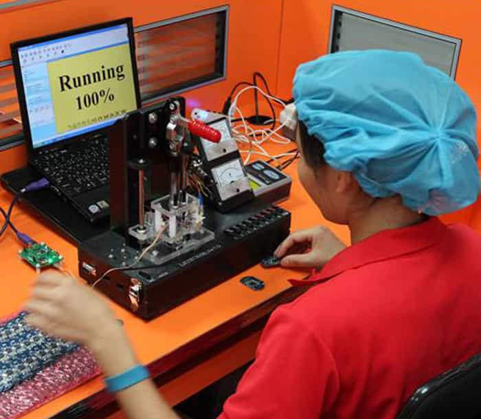
8) FCT- Functional Test and System Test
The FCT function test is usually used on some more complicated circuit boards. The circuit boards that need to be tested must be soldered and passed through some specific fixtures to simulate the circuit boards’ real usage scenarios. It would be best if you placed the circuit boards in this simulation. In the scene, after turning on the power, observe whether the circuit board can be used usually. This test method can accurately determine whether the circuit board is normal.
9) Reliability Test
The reliability test verifies the PCBA under the environmental influence. The cost of reliability testing is not high, mainly to verify the performance of component welding. The disadvantage is that the test time is longer.
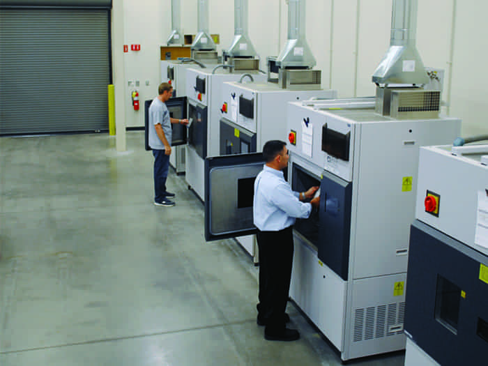
10) Burn-In Testing
As the name suggests, burn-in testing is a more intense type of testing for PCBs. It’s designed to detect early failures and establish load capacity. Because of its intensity, burn-in testing can be destructive to the parts being tested.
Burn-in testing pushes power through your electronics, usually at its maximum-specified capacity. The power is run through the board continuously for 48 to 168 hours. If a board fails, it is known as infant mortality. For military or medical applications, boards with high infant mortality are clearly not ideal.
Burn-in testing isn’t for every project, but some applications make a lot of sense. It can prevent embarrassing or dangerous product launches before they reach customers.
Just remember that burn-in testing can shorten the product’s lifespan, especially if the test puts your board under more stress than it’s rated for. If few or no defects are found, it’s possible to reduce the testing limit after a shorter period to avoid over-stressing your PCBs.
Recommended PCB Assembly Services
PCB and PCBA Testing videos
How To Test a PCBA?
Flying Probe Test for PCBA
Electrical Testing-Flying Probe Test for PCB