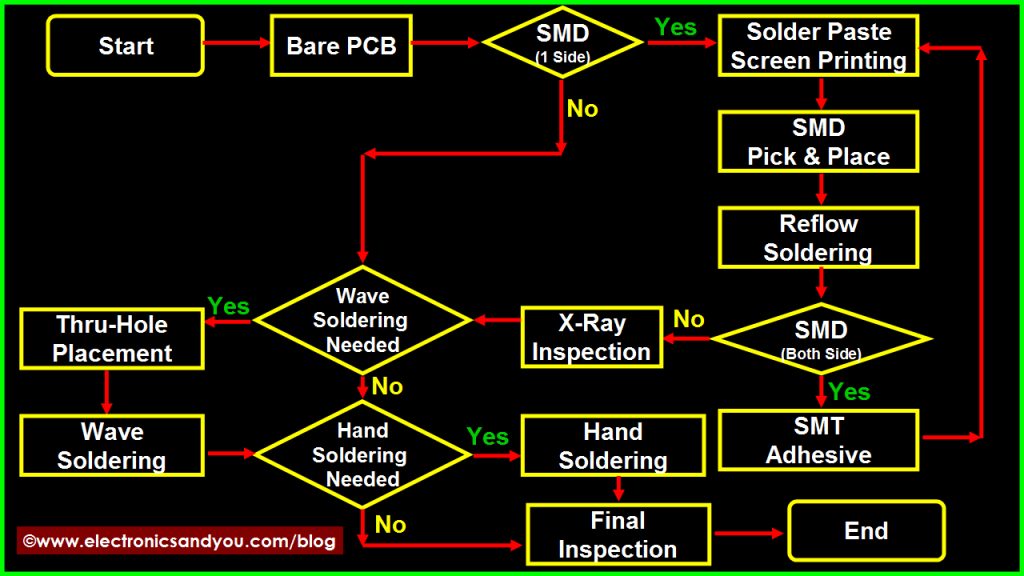
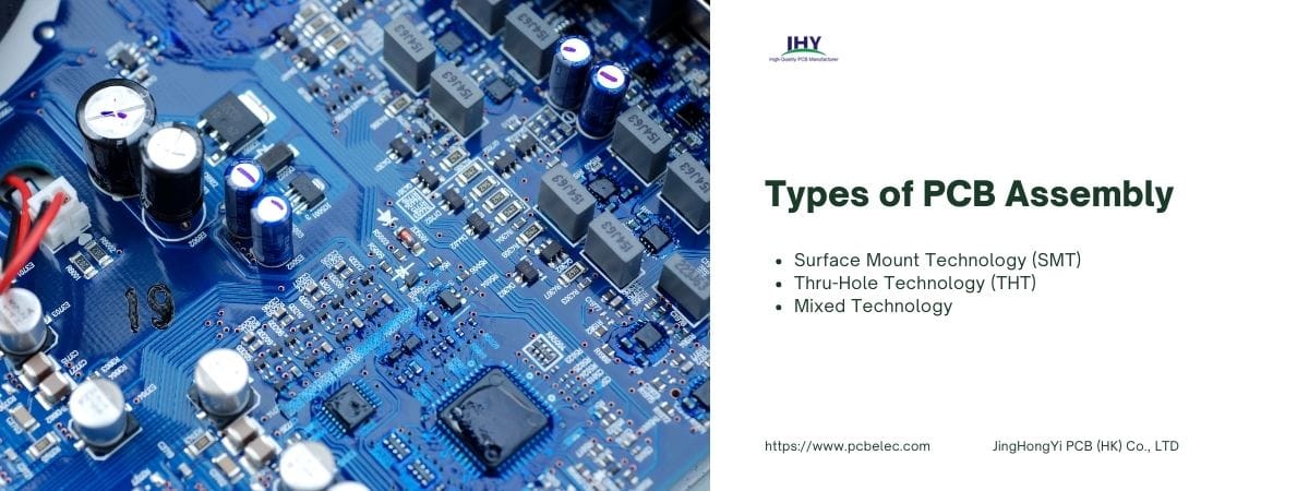
Thru-Hole Technology
Thru-Hole Technology or THT is the oldest method of PCB Assembly. In this method, the components are mounted on the board with the help of leads. These leads are inserted into the drill holes, and then the leads are soldered using manual soldering or wave soldering. As we need to drill holes in THT, it is not suitable to perform on double or multi-layer PCBs. It is very difficult to drill holes in a multi-layer PCB and maintain its design and accuracy.
Modern technology and appliances now use and require SMT, and SMT has replaced it in various applications. But THT can never be eliminated; it is because certain applications require THT and are still replaceable. For example, if there is a simple task to perform like a digital clock or a simple toy, why would anyone use SMT when it can be done using THT. This is the reason THT is still used today in different applications and circuits.
THT has some advantages over SMT. It includes the ease of replacing and adjusting the position of components. Moreover, THT is highly used when it comes to PCB testing and prototyping. It has high durability. It has more heat resistance and stress tolerance than SMT and also has better mechanical strength. But sadly, THT has lower efficiency than SMT and has limited or restricted PCB designs.
Type of Soldering
We know that THT assembly requires soldering because it uses leads to mount the component on the bare board. The leads are on the lower surface of the board that needs soldering. Manual soldering and wave soldering are used for soldering these leads and making connections so that circuit can function properly. Let us see what these soldering methods are and what makes them different from each other.
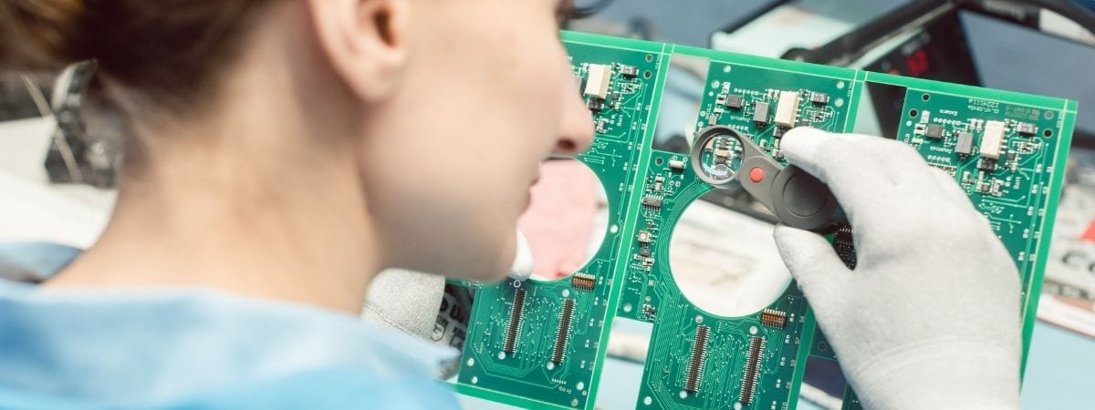
1- Manual Soldering
It is the conventional and oldest method of soldering. Here, a single person is responsible for putting a component, mainly PTH components, into a specific and designated hole and soldering it. Then the PCB is moved to another station where another person is responsible for putting a PTH component in the hole and soldering it. It is a lengthy process and consumes a lot of time. This is the reason it is very less likely to be used in industries with high production requirements. However, some components still need manual soldering.
2- Wave Soldering
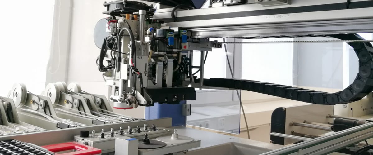
Wave soldering is a modern method of soldering, and it has replaced conventional manual soldering. Here, the person only needs to place the components in PTH holes, but it can also be done by a machine. After placing the components, the board is then put on a conveyor, where it is led to a hot oven where the solder melts. PCB goes through a wash of molten solder waves on the lower surface. This wash solders all the pins from beneath. However, wave soldering cannot be applied to a double-sided PCB. If it is applied, then all the electronic components on the lower side will not work. It is why manual soldering is not obsolete and still being used in the industry.