
X-ray Inspection in PCB Assembly
The Importance of X-ray Inspection in PCBA
Home » PCB Board Testing and Inspection » X-ray Inspection in PCB Assembly
Preface: The rapid development of high-density packaging technology has already brought up the new challenge to testing technology. For replying challenges, new testing technology continuously appears; X-ray inspection is one of them; it can be used to control the quality of BGA soldering and assembly. Now X-ray inspection systems have been specifically designed for PCB Assembly and semiconductor industries offering a high resolution. X-ray systems not only within failure analysis laboratories but also within the production environment. This article introduces the theory and the application of X-ray inspection, indicates that X-ray inspection is a necessary method to guarantee the quality of electronics assembly.
Contents
What is X-ray Inspection in PCB Manufacturing?
X-ray inspection technology, commonly referred to as automatic X-ray inspection (AXI). These are special rays with powerful electromagnetic waves and extremely short wavelengths. The wavelength is way shorter than that of visible light, less than 10 nanometers. What makes x-ray find application in an industrial setting is the high penetrating power. An X-ray can penetrate a substance that visible light cannot detect. Today, X-ray inspection is widely used in many fields such as medical, industrial control and aerospace. As for PCB inspection, X-rays are used extensively in the PCB assembly process to test the quality of the PCB, which is one of the most important steps for a quality-oriented PCB manufacturer.
Some of the characteristics of X-rays are:
- Ionization
- Penetration
- Heat
- Refraction
- Fluorescence, etc.
AXI features some advantages as a type of structural test and inspection:
- Some defects can be found in the early stage of the printed circuit board assembly process;
- It is contributive to the cost reduction of defects;
- It stops defects from flooding among remaining PCB assembly or even clients’ practical projects.
PCB X-ray inspection is one of the breakthroughs in manufacturing. It allows designers and engineers to detect defects. The defects could be in several parts of their components like BGA, soldering, and CSP defects.
In recent years, area array packages including BGA and QFN, flip chip and CSP are widely used in various fields such as industrial control, communication, military, aviation, etc., making the solder joints hidden under the package. This fact prevents traditional inspection equipment from playing its perfect role in PCB inspection.
In addition, due to the appearance of surface mount technology (SMT), which makes packages and leads smaller, traditional inspection methods (including optics, ultrasound, and thermal imaging) are not sufficient because PCBs have higher density and their solder joints Hidden, loopholes or blind holes.
In addition, with the increasing miniaturization of semiconductor component packages, the trend of miniaturization of current and future components cannot be ignored while considering X-ray inspection systems. Compared with other inspection methods, X-rays can penetrate into the inner packaging and check the quality of the solder joints.
During the mass production of various PCB prototypes and complex Printed circuit boards, x-ray inspection comes in. With this technology, PCB manufacturers can supply PCB components of high quality to customers.
That’s why X-ray is so important in PCB assembly.
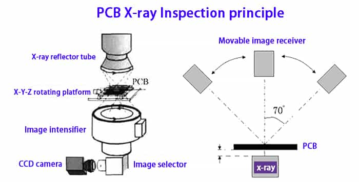
X-Ray Inspection Principle
What makes x-ray find application in an industrial setting is the high penetrating power. An X-ray can penetrate a substance that visible light cannot detect.
Under high pressure, X-ray emits light that can penetrate the test subject. This reveals an image with various thickness and density. The image quality helps explain the quality of the joint.
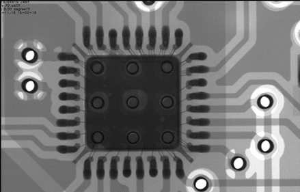
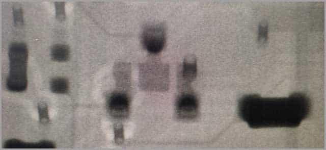
One of the unique advantages of X-ray materials is that they absorb X-rays that are proportional to their atomic weight. All materials absorb X-ray radiation differently according to their density, atomic number, and thickness. In general, materials made of heavier elements absorb more X-rays and are easier to image, while materials made of lighter elements are more transparent to X-rays. Therefore, a general X-ray inspection image is shown in FIG. 1.
From the figure, a dark black image refers to a material composed of heavy elements, and a transparent or relatively white image refers to a material composed of light elements. Therefore, X-ray inspection is a good way to inspect hidden defects, including open circuits, short circuits, misalignments, lack of electrical components, etc.
How Does PCB X-ray Inspection Work?
Many industrial processes use an x-ray to inspect the internal layout of the PCB and other components. It helps determine the efficiency and identify faults in the design. This happens during the initial manufacturing stage and testing.
During testing or inspection, the designer positions the component between the X-ray machine and the detection component. The penetrating power of x-rays depends on some factors like:
- The energy of the x-ray
- The density of the material
- The material’s nuclear charge
Before the inspection, an X-ray machine can be set such that it considers the above factors. As a result, the detection component will give out a visual element of the filmed part. The film can either be a modern digital media or a traditional radiographic film.
The modern digital media could be direct digital arrays or phosphor screens.
We prefer modern digital media due to many advantages like:
- Impressive resolution
- High flexibility
- High contrast
- Saves time and conserves resources
Many X-ray systems have a fixture that allows user to hold and manipulate the subject. This allows the engineer to access the issue from a different angle. As the X-rays journey through the test subject, the rays will reduce in quality and intensity. This is due to the varying density in the test subject. The effect of this is various shades of light and dark areas on the detection surface.
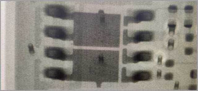
This explains why a crack or crevice present in a solder ball will show up quickly in an x-ray. Its visibility is because the solder has a greater density compared to air present in the aperture. As a result, the reduced density weakens the intensity of the x-rays. You will see the solder ball as the light area on the X-ray result since the density weakens significantly. The aperture will also show up as a dark crack where the x-rays’ thickness was reduced experienced a little reduction.
Automatic X-ray Inspection Equipment
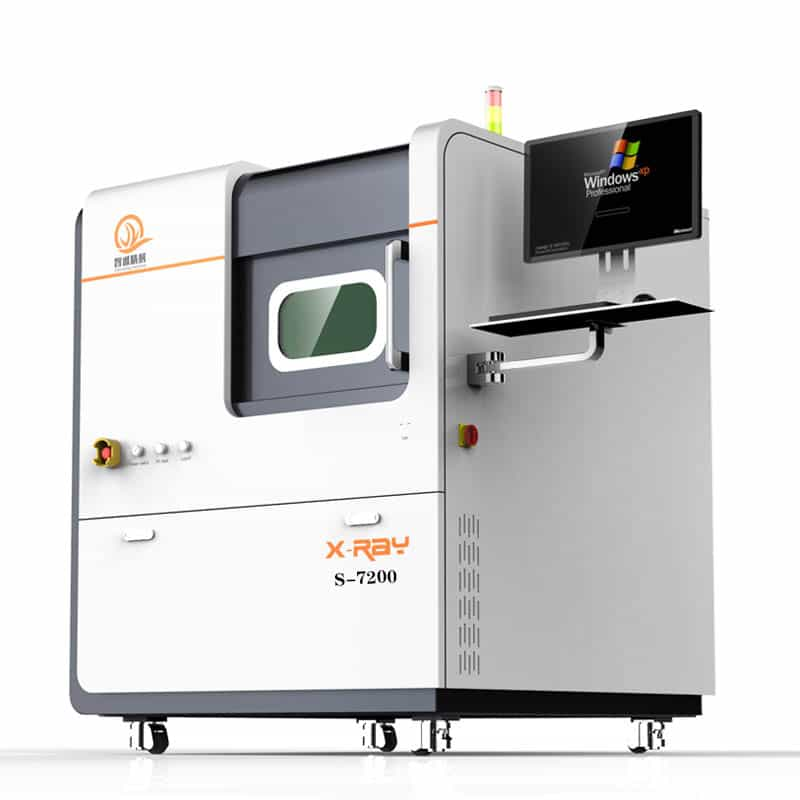
There are two primary types of equipment used for the X-ray inspection system for CSPs and BGAs. These are the 2D (two dimensional) system and the 3D (three dimensional) system. JHYPCB uses model VIEWX2000, responsible for inspecting PCBA manufacturing defects including opens, shorts, insufficient solder, excessive solder, missing electrical parts, misaligned components, solder voiding, etc.
2D X-ray Transmission system:
This process generates x-rays at a single point. The x-rays then pass through the PCBA. This process triggers an image on the electronic detector. You will get the picture in a digital format on a computer after it completes the analysis.
Designers use this technique for single-sided boards and assemblies where accuracy is of utmost importance. The medical field uses this principle where an X-ray to inspect the condition of a fractured bone. Similarly, the 2 D x-ray system displays the entire component’s 2D image from both sides of the PCB.
3D X-ray Transmission system:
Engineers use 3D X-ray transmission for complex double-sided PCBs. 3D X-ray inspection needs two essential components: the detector and the X-ray source. The sensor undergoes a 180-degree circular movement.
The idea of a 3D X-ray transmission is to generate images of various cross-sections. It does this by reconstructing series of 2D images. The X-ray focuses on a single feature at once. It blurs the components of other features like soldering joints. As a result, 3D X-ray transmission allows you to dwell on a specific element of interest at a time.
All X-ray inspection equipment, whether 2D or 3D, have the following characteristics:
- There is an X-ray tube in the equipment to generate X-rays.
- A sample operation table carries the sample to move so that different parts of the sample can be detected, and the magnification can be adjusted, and the oblique angle can also be observed.
- An image receiving device can capture the X-ray passing through the sample and convert it into a good image that can be presented in front of the user’s eyes.
Applications of X-ray Inspection in PCBA
Thanks to an improvement in technology, many industries use automated x-ray inspection. There are manufacturing processes where safety is paramount. As a result, there must be thorough checks of all parts that they produce.
These apply to industries to detect impurities (glass, metal, sand) in processed foods. It also helps optimize processing and boost yields. For instance, food industries use it to determine the size and the perfect place for better slicing patterns for holes in the cheese.
When manufacturers want to produce an item in mass, X-ray inspection also applies. In the manufacturing of electronics, for instance, X-ray inspection can help detect defects early. As a result, manufacturers will not use a defective part in mass production. This leads to significant cost savings. It also saves companies from a soiled reputation that could arise from mass-producing faulty outputs.
In summary, here are the benefits
- PCB Manufacturers get feedback on their products as early as possible. This allows them to know if the materials are compromised. They can also detect if the integrity of process parameters gets compromised.
- Designers will not have to build on defective parts. As a result, they get to save unnecessary costs.
AXI Vs. AOI PCB Inspection
Belonging to the same structural test and inspection category, AXI shares the same principle with AOI; the inspection is carried out by capturing images. The difference between them lies in the source in that AOI depends on a light source to capture pictures while AXI on X-ray. Materials absorb X-rays according to their atomic weight proportion. Fabrics made of heavy elements get more X rays absorbed while those made of light elements get fewer. As a result, materials soaking more X rays are displayed more obvious or darker in their images than those absorbing fewer rays. When it comes to PCBA, solder joints are made of materials with heavy elements. In contrast, other parts such as most packages, silicon ICs and component leads are made of materials with delicate features. Therefore, high-quality solder joints should look darker or more obvious on images than other parts.
Based on its working principles and capabilities, AXI is applied to test circuit boards containing components with array-style packaging or adequate pitch packaging, including BGAs, CGAs (Column Grid Arrays), CSPs (Chip Size Package), etc. AXI is usually placed in the assembly process, just after the last soldering, no matter-wave soldering or reflow soldering. Furthermore, AXI is usually applied coupled with the boundary-scan test, ICT, and functional test to obtain optimal inspection results.
Although AXI and AOI have the same working principles and play similar roles in PCB assembly production lines, defects they can detect differ to some extent. The following table shows the comparison between AXI and AOI in terms of their inspection coverage.
| Inspection capability Comparison Between AXI and AOI | |||
| Defect Type | AXI | AOI | |
| Components | Lifted lead | Yes | Yes |
| Faulty component | No | No | |
| Missing component | Yes | Yes | |
| Incorrect component value | No | No | |
| Misaligned/Misplaced component | Yes | Yes | |
| Soldering | Open circuits | Yes | Yes |
| Solder bridges | Yes | Yes | |
| Solder shorts | Yes | Yes | |
| Insufficient solder | Yes | Yes | |
| Solder void | Yes | No | |
| Excess solder | Yes | Yes | |
| Solder quality | Yes | No | |
| BGA and CSP | BGA Shorts | Yes | No |
| BGA open circuit connetions | Yes | No | |
Conclusion
Application of X-ray Inspection in PCB Fabrication and assembly
- The use of X-ray inspection is to detect various faults and defects in the manufacturing of PCB. Here are some flaws PCBs help take care of the following:
- Soldering Defects: With X-ray inspection, manufacturers can detect countless soldering problems. Examples are solder bridges, open circuits, excess solder, cold soldering, poor soldering, insufficient soldering, solder shorts, solder voids, etc. They can even access the soldering quality.
- Component Defects: X-ray inspection also helps check component defects like lifted leads, faulty components, misplaced components, and missing components.
- CSP and BGA defects: The complexity of various BGA components and CSP components makes them invisible to the naked eyes. With advanced X-ray inspection, designers can detect defects like open circuit connections, soldering bumps, and BGA connections.
X-ray inspection technology has brought new changes to production inspection methods. It is currently the best choice for manufacturers who are eager to improve further the level of PCB fabrication and assembly production technology, improve production quality, and timely find faults in electronic assembly as a breakthrough. With the development trend of PCB manufacturing and assembly in the future, other assembly fault detection methods are challenging to implement due to their limitations. X-ray inspection equipment will become the new focus of SMT PCB assembly production equipment in the future and will play an increasingly important role in the production field!
Not only does X-Ray inspection detect issues in PCB assembly, but the analysis of an X-Ray image can help to determine the root cause of a given defect, such as insufficient solder paste, skewed part placement, or improper reflow soldering profile. This technique contributes greatly to JHYPCB’s Quality Management strategy for complex components.
Advanced Learning:
- Why is prototype PCB manufacturing so important?
- Reasons for Rapid PCB Prototype Manufacturing
- SMD LED PCB Board Assembly, LED Light Circuit Board Assembly Service
- Fast Prototype PCB Assembly Service
- Low Volume And Quick Turn PCB PCB Prototype Assembly Services
- What is the difference between wave soldering and reflow soldering?
- How to Store PCB and PCBA?
- How long can PCBA finished products be stored?
- The Production Process and Specifications of PCB SMT stencil