
Single-Sided PCB, Single Layer PCB Complete Introduction and Manufacturing Services
The Most Important Things You Need To Know About Single-layer PCB
Home » PCB Manufacturing » Single Layer PCB
Single Sided PCB, also known as a Single Layer PCB, is a type of PCB that comes with only one layer of conducting material on one side of the board, and the other is used for mounting electronic components.
Single-Sided PCBs are the starting point of Printed Circuit Board technology. Because of their simple design and low cost, they still play an essential part in the electronic industry.
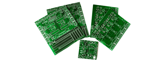
Single Layer PCB Manufacturer - JHYPCB
A detailed introduction to single-sided circuit boards
Single-Layer PCB Definition
What is a Single Layer PCB?
When it comes to PCBs, they are named single-layer, double-layer, and multilayer PCBs. The number of layers in a PCB is the number of conductive or copper layers it has. PCBs also have other layers, such as the base layer, dielectric layer, solder mask, and silkscreen; however, the number of layers only represents the number of copper/conductive/circuit layers. Thus, a PCB with one conductive layer to create a circuit is known as a Single Layer PCB.
A Single Layer PCB is the simplest PCB as there is only one conductive layer. It is widely used in dozens of applications where we need a compact circuit. Among all types of PCBs, single-layer PCBs are preferred and the most purchased. Designers go for double-layer or multilayer PCBs when the circuit is quite complex and cannot be implemented on a single-layer circuit. Otherwise, a single-layer PCB is the first choice for any device, product, or project.
Express 1 Layer PCB Fabrication Service
Types of Single Layer PCB
It is a single-layer PCB made up of a rigid material such as fiberglass (FR-4). These PCBs are inflexible and prevent the circuit from bending. They are used in calculators, power supplies, etc.
It is a single-layer PCB type made of a flexible material instead of a rigid one. It has many advantages over a single-layer rigid PCB, but its fabrication cost is very high.
Rigid-flex PCBs combine the rigidity of rigid PCBs with the flexibility of flexible PCBs and are widely used in many applications. Single-sided rigid-flex PCB is one of them.
It is a single-layer PCB used for high-frequency circuits. These PCBs are made of unique material. Common ones are Rogers, Taconic, Panasonic, Isona, Shengyi, etc.
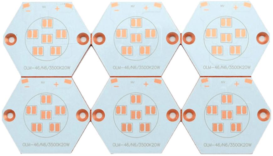
It is a type of single-layer PCB made from aluminum substrate. The design of this PCB is almost the same as copper-backed PCB, but the only difference is aluminum substrate is used instead of copper.
Single Layer PCB Benefits
What are the advantages of Single Sided PCB?
- Simple Design: The design of a single-sided PCB is quite simple. There is only one conductive layer, so it is easy for the designers to create a design. There are fewer errors in the designing process, and the PCB is more likely to offer the desired results even in the first prototype.
- Easily Available: Single-sided PCB is quite easy to manufacture as it has a basic design. You can easily find a single-layer PCB manufacturer in your city or country. All PCB manufacturers offer this service, so you can easily order anyone.
- Low Cost: The cost of a single-layer PCB is lower than a multilayer PCB. It does not require high-end pieces of machinery as in other types of PCB. If you order in bulk, the price of the PCB is further reduced. A single-layer PCB is the best choice if you want to save costs.
- More Reliable: The design of a single-layer PCB is simple, so it is more reliable. There are fewer chances of errors and faults. It offers excellent performance and high reliability. The long-lasting operation of the board and components is also ensured.
- Easy Testing and Repairing: The testing of a single-layer PCB is easier than a multilayer PCB. The PCB can be easily checked by AOI, or X-ray inspection can be used in the case of BGA components. If there is any fault, it can be traced easily. Moreover, repairing a single-layer PCB is easier and simpler.
What are the disadvantages of Single Layer PCB?
- Large Size (Extra Dimensions): In the case of multilayer PCBs, the circuit is distributed in all layers. Therefore, the circuit does not take much space on the board. Moreover, the circuit looks clean. On the other hand, the circuit of the single-layer PCB is present in one layer only. Thus, the circuit takes more space on the board; the board will be larger.
- Cannot Deal with Complex Designs: If the requirement of your project is a complex circuit, you cannot implement it on single-layer PCBs. There are some limitations, so not everything can be achieved by a single-layer PCB.
- Slow Speed: Single-layer PCBs offer slow speed and transmission as compared to multilayer PCBs. If you need high-speed, you need to go for a double-layer or multilayer PCB.
- High Weight: The increased size and high component count ultimately increases the weight of a single-sided PCB.
Single-Sided PCB Applications
What are single-sided PCBs used for?
Single Layer PCBs are very common, and we are usually surrounded by dozens of devices that use single-sided PCBs. Some of the common devices that we see are,
- Vending machines
- Camera systems
- Surveillance
- Calculators
- Printers
- Solid-state drives
- Coffee makers
- LED lighting
- Packaging equipment
- Sensor products
- Power supplies
- Relays
- Radio and stereo equipment
- Timing circuits
Single-sided aluminum substrate and single-sided copper PCB are our most common single-sided circuit board applications.
There are dozens of applications where a single-layer PCB is used. As long as the desired results can be achieved by the single conductive layer, it is recommended and cost-effective to select a single-layer PCB instead of a multilayer PCB.
Almost all simple devices that we use contain a single-layer board. For complex applications and circuits, it is necessary to have more layers in the PCB.
Single-sided PCB Design
Single-sided PCB Stack up
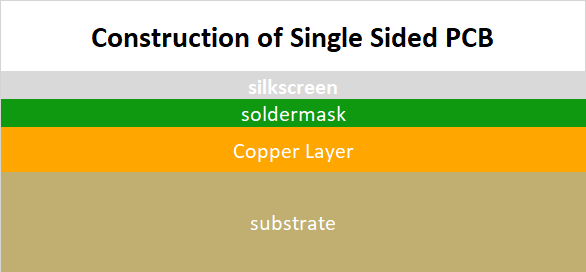
The stack up in a single-layer PCB is quite simple. There are only two primary layers, but if we count the total number of layers, including the solder mask, surface finish, and silkscreen, then there will be more layers in total. However, the important layers are only two layers: The conductive Layer and Base Layer.
- Conductive Layer
The conductive layer conducts the signals and transmits the electrons. There is only one conductive layer in single-layer PCBs, and it is usually made of copper. Other materials, such as Gold and Silver, can also be used as a conductive layer, but Copper is the most cost-effective and feasible.
- Base Layer
The base layer of PCBs can vary. The commonly used base layer is FR-4; however, metals are also used as a base material. The base layers provide a platform or base to all other layers. This is the foundation layer on which copper layer, silkscreen, and other layers are applied. PCBs can further be classified on the basis of the base layer.
Related Reading: Standard PCB Thickness—All You Need To Know
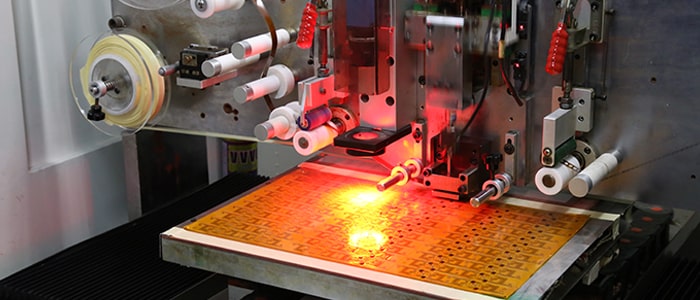
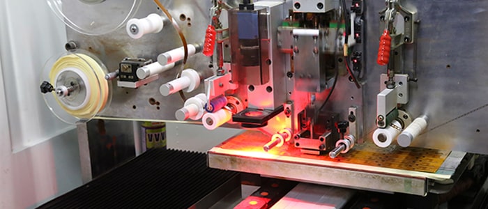
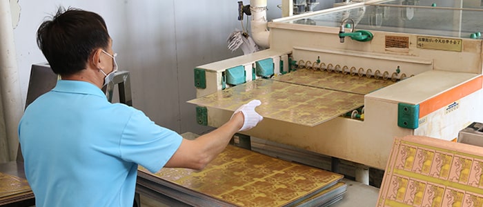
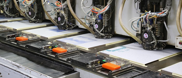
Single Layer PCB Manufacturing Process
How Single Sided PCB is Manufactured?
The manufacturing of a PCB is a long process. The PCB that looks like a simple board goes through more than a dozen machines to create a final product. For the ease of customers, PCB manufacturers define the process in simple words.
Single-sided PCB Manufacturing Process Flow Chart
Cutting – Cleaning – Drilling – Cleaning – PTH – Panel – Plating – Cleaning – Photolithography – Image Transfer – Inspection – Copper/Tin – Plating – Coating – Removing/Etching/Tin – Removing – Inspection – Cleaning – Solder – Mask – Exposure/Develop/Inspection – Prepreg – Screen – HASL – Conformal – Coating – Post – Soldering – Cleaning – Test – Final Inspection – Packing
Customers place orders and provide the important files required to create a PCB. They provide Gerbers and other essential files. PCB designers usually do not understand the nitty-gritty of the manufacturing process. They just create a design to get the desired results; however, it is important to understand the manufacturing problems that can be due to design. For this purpose, we run a DFM check on the files. Our experts look at the files and make sure it is according to the manufacturing requirements. If there is an issue with the design, we correct it or inform customers in the case of severe problems.
We offer a free DFM check at JHYPCB. If this check is ignored, there can be possible delays and unwanted errors in the production. Therefore, it often delays the final shipment. For timely delivery, a DFM check is more than essential. Once the PCB files are ready for the manufacturing process, the experts forward them to the next department.
According to the requirement of the buyer/customer, the base of the PCB is selected. Usually, it is FR-4, but it can be PTFE, CEM, Aluminum, Copper, or any other material suitable for the project. The board is procured and then cleaned. It is cut according to the standard size that the machines can accept. There can be one or multiple PCBs on a single board.
Drilling is done for lead components, such as BGA packages. If there are such components on the board, drilling is necessary. It can also be done to fix components, heat sinks, and other devices. Another important use of drilling is the connection of layers. If there are multiple layers, they are connected through vias.
After drilling, there is debris on the board. The board is cleaned again before proceeding to the next step.
The board is then passed through a series of chemical baths for electroplating. Copper is deposited in the vias to create a connection between the layers where required. The boards are dipped into baths for a certain time and then taken out for the next stage of the chemical bath.
Copper plating is an important process. In this stage, a certain thickness of copper is applied to the board. The thickness of copper depends on the customer’s requirements.
For creating the circuit pattern on the PCB, a photo-resistive film is applied. All this work is carried in a room where white light cannot enter.
After applying the photo-resistive film, there are separate films that contain the circuit diagrams. These films are then placed over the board, and the board passes through a UV chamber. Through the passage of UV light, the photo-resistive film hardens on the surface of the board and creates the pattern required.
Due to the presence of the circuit-printed film on the board, only the circuit is hardened, and the rest of the area remains the same. When we see the board at this stage, it has the complete circuit in blue. After this process, the unwanted photoresist is removed.
Etching is the process of removing the unwanted copper from the PCB. Copper should stay only on the circuit, and the rest of the copper must be removed. For this purpose, the copper on the board is reacted with a powerful alkaline solution, which is a solution of various compounds, such as copper chloride, hydrogen chloride, and hydrogen peroxide. The solution removes the unwanted copper, and the circuit that is hardened using UV remains the same.
Automatic Optical Inspection (AOI) is an excellent way to find faults on the PCB. In this inspection method, there are several cameras at different angles. The cameras take pictures of the PCB and compare them with the files. If there is any problem, the PCB is separated. This inspection is quite fast, and it detects opens, shorts, solder bridges, low solder, and other problems.
Advanced Learning:
A solder mask is a thin polymer layer applied over the PCB. The buyer can choose the color of the solder mask. The color could be Green, White, Blue, Red, Black, and Purple.
The solder mask not only gives a nice appearance to the board but also prevents the formation of solder bridges. It is possible that the solder pads with low spacing can create a short circuit, but due to the solder mask, it never happens. It also protects the board from corrosion and oxidation.
Silk Screen is just like printing labels on the board. This helps in manual assembling and repairing. It can also be used to find the wrong placement of components.
The surface finish is quite essential for a PCB. The circuit is made of copper, and it can undergo oxidation and corrosion quickly. It is necessary to protect the circuit, and for that purpose, a surface finish is used.
Many types of surface finishes are available, such as HASL, LF HASL, OSP, ENIG, ENEG, ENEPIG, etc. The buyers can choose any surface finish according to their requirements.
This is the final test in which probes check the circuit. Voltage is applied using these probes to check the opens and short. Once the whole board is tested, it goes for final cleaning, inspection, and packaging.
Learn more about what is Flying Probe Test?
Base Material for Single Layer PCBs
There are various base materials available for PCBs, and the buyer can easily pick any of them according to the requirement of the project. All bases have distinct characteristics, features, pros, and cons, so you need to decide which one is the best for your application.
The commonly used and demanded materials for Single Layer PCBs are,
- FR-4
- CEM
- Teflon
- Polyimide
- Metal
Learn more PCB Materials
FR-4 is the most commonly used PCB material. It is used in almost all types of standard environments and projects where it can perform well. It is made of prepregs that are created from fiberglass. The prepreg sheets are impregnated with the help of epoxy resin. Therefore, it is commonly known as glass-reinforced epoxy laminate.
FR-4 is also available according to the temperature it can bear. High-Tg FR-4 boards are available for applications where high-temperature stress is expected. These can even bear temperatures up to 200°C.
This material is widely used as it is cheap and excellent for most of the requirements. It has high dielectric strength as it is itself an insulator. Moreover, it is lightweight and temperature resistant. Due to its features and low cost, it is commonly used in the devices that we use in our daily lives.
FR-4 PCB boards are not suitable for high-frequencies and high temperature and pressure stress. In such conditions, metal core PCBs are considered.
Advanced Learning:
CEM stands for Composite Epoxy Material. CEM-1, CEM-2, CEM-3, and some other variants are available. These variants of CEM are made of paper impregnated with epoxy. They also have a layer of glass fiber.
CEM is a bit cheaper than FR-4 and is used in many applications. It is not as strong as FR-4 boards because of its construction. So, it cannot be used under high-pressure stress.
PTFE is the best choice for high-frequency applications. Common PCBs, such as FR4, cannot offer good performance on high frequencies, which is why PTFE is preferred. It works perfectly well in the case of high-speed electronic devices.
PTFE is a hard synthetic resin, so it can bear more temperature stress and pressure stress. It can have a high Tg value of up to 280°C. It also offers excellent dielectric properties.
PTFE is definitely better in many aspects compared to FR-4, but all these things come at a very high cost.
Polyimide is a flexible material; therefore, it is used to make flexible and rigid-flex PCBs. Due to its flexibility, it is suitable for any type of space, whether small or complex. It can bear more stress as it is flexible. It offers excellent heat resistance and mechanical strength.
Metals are also used as the base material. Mostly, aluminum and copper are used, and sometimes iron is used in the making of the base material.
As the base is of metal, such PCBs are pretty strong. They can bear heavy pressure and high-temperature stress. On the other hand, FR-4 PCBs can bend under high temperatures, and they can break under high pressure. Moreover, FR-4 PCBs can also deteriorate with time.
Metal core PCBs can dissipate heat 6-9 times better than FR-4 and similar materials. Due to excellent heat dissipation properties, the components remain cool and last for a long time. Metal core PCBs have solved all problems associated with FR-4 and other common materials, but they are pretty expensive.
Advanced learning:
Single Layer PCB Thickness
What is the Single-sided PCB Thickness?
Typically, the industry standard for PCB thickness is about 0.063 inches, which translates to about 1.57mm in metric units.
Today, PCB thicknesses range from 0.2032mm to 6.096mm.
The thickness of the printed circuit board affects the performance, function, and installation of the PCB. We need to choose and determine the most suitable PCB thickness for you according to the actual application and the size of the installation area.
PCB thickness varies. Usually, rigid PCB is thicker than flexible PCB; multilayer PCB is thicker than single-sided and double-sided PCB. Some devices require thicker PCBs, while others may require thinner PCBs.
Factors that determine PCB thickness include PCB weight, number of layers, size, copper thickness, trace thickness, board manufacturing process, flexibility, working environment, signal type, via type, etc.
As people demand smaller and smaller electronic products, PCBs are also shrinking. This also requires the circuit board to be light and thin to fit inside the device.
Single Layer PCB Price
Cost of Single Layer PCB
The Single Sided PCB Price depends on various factors. Some of the factors are primary, while some are secondary.
The first thing is the type of base material. You can choose metal, FR-4, PTFE, or any other material. Along with the type of the material, the thickness of the base also matters. Then, it is important to measure the size of the board and circuit. These two are the most important factors in PCB production. After that, you can consider the surface finish, copper thickness, via filling, tracing, holes, and some other factors.
Buyers also require PCB assembly services. In this case, you need to add the cost of the components and testing.
The cost of the PCB also depends on the order. High volume orders will give you less cost per piece. So, you can also reduce the cost if you have a bulk order.
What are the factors that affect the price of single-sided PCB?
| Primary or Fixed Production Costs | Secondary or Dependent Costs | Overhead Costs |
|---|---|---|
| Board Size | Tooling | Facility |
| Number of PCBs produced in a production run | Layout – trace design, hole size, and hole count | Labor – salaries and benefits |
| Number of layers beyond double-sided | Lamination | Equipment |
| Lead time | Change needed from mechanical drill type to laser drill type | Raw materials |
| Hose size and count | Quality assurance | Chemical processes |
| Material type and thickness | Via fill | Waste water treatment |
| Layout | Fabrication | Regulatory permits |
| Finish | Production delays due to design or fabrication changes | |
| Production failure due to bad design or flawed methods |
Single-sided vs Double-sided PCB: How to Choose?
Single-sided and double-sided PCBs are distinguished according to the number of conductive layers, and they are all made of FR4 and copper foil.
Double-sided PCBs enable more complex circuit designs than single-sided PCBs, but sometimes single-sided PCBs may be more suitable for your actual needs.
In terms of price, producing single-sided PCBs is more economical than double-sided PCBs.
Read this article to learn more about the difference between single-sided and double-sided PCBs.
Single-sided PCB vs. Multilayer PCB: What is the difference between?
1. The components of the single-sided circuit board are on one side of the board, and the circuit is on the other side of the board. Single-sided circuit boards are simple to manufacture and low cost and are only suitable for simple electronic products.
2. There are three or more layers in the multi-layer PCB, and the conductive pattern layer is separated by insulating material between two layers and then formed by pressing. Multilayer PCBs are widely used in more complex electronic products, providing high-capacity, high-speed, and multi-functional support for electronic products.
3. The single-sided PCB has only one side with the circuit, and the holes on the board are all non-metalized holes, and no electroplating is required in the single-sided PCB manufacturing process. The holes on double-sided and multi-layer PCBs are divided into metalized holes and non-metalized holes, and an electroplating process is required in the production process of the board.
4. The most essential difference between single-sided PCB and multi-layer PCB is the number of circuit layers.
Single Layer PCB Manufacturer
Buy Single Layer PCBs from JHYPCB
JHYPCB is one of the leading PCB and PCBA service providers in China. We have a large facility where we can handle small to large volume orders. We can provide any single-layer PCB, including metal core PCB, high-frequency PCB, flexible PCB, HDI PCB, impedance control PCB, and heavy copper PCB. There is no limitation on order; you can order one PCB as well. We offer quick prototype and assembly services under a strictly controlled management system. We are ISO, UL, or RoHS certified so that you can order with confidence.
For more information and details, feel free to contact our 24/7 customer support team.
Get Free Quote or contact JHYPCB to learn how we can help you with your application.
Single-sided PCB FAQs
Double-sided PCB is one of the most produced and used printed circuit boards today. The difference between a double-sided PCB and a single-sided PCB is that a double-sided PCB has traces on both the top and bottom sides. Double-sided PCBs can also mount electronic components on both sides. Using double-sided PCB can realize a more complex electronic circuit design, which is more conducive to manufacturing more complex technical applications and electronic products.
Components can be installed on the breadboard at will, plug, and play, and experimental tests can be performed. After the test is completed, the components can be removed; and the breadboard can be reused。 But the single-sided PCB needs to solder or mounted the components before they can be used and is Not reusable.
PCB, that is, printed circuit board, can be divided into single-sided PCB, double-sided PCB, and multi-layer PCB according to the number of layers; according to hardness, it can be divided into rigid PCB, flexible PCB, and rigid-flex PCB; according to the conductivity of holes, it can be divided into Through-hole PCB, blind-hole PCB, buried-hole PCB, plated-through-hole PCB, and non-plated-through-hole PCB.
The number of PCB layers is mainly determined by functional requirements, which are embodied in:
- Application scenarios
- Signal transmission speed
- Project budget
- Lead time
- Component pin density
- Top Layer: Routing layer, single-sided PCB does not have this layer
- Bottom Layer: the bottom copper foil routing layer
- Top/Bottom Solder Mask Layer: Top/Bottom Solder Layer generally uses a green solder mask to prevent tin on copper foil and maintain insulation.
- Top/Bottom Solder Paste Mask Layer: This layer is generally used for solder paste during the SMT reflow process of SMD components
- Top/Bottom silkscreen Layer: printing various logos such as component tag numbers, characters, trademarks, etc.
- Midlayers (Signal Layer): mostly used for multi-layer PCB, that is, the actual copper layer
- Mechanical Layer: Define the appearance of the PCB board. Mechanical layers have no electrical properties
- Drill Layer: Divided into Drill Grid and Drill Drawing. Drill Layer is used to provide drilling information during circuit board manufacturing
- Keep out layer: used to define the boundary of the routing layer. After defining the forbidden wiring layer, the routing with electrical characteristics cannot exceed the boundary of the forbidden wiring layer in the subsequent wiring process.
- Interna Plane: These layers are usually connected to ground and power and become power and ground planes, only present in multi-layer PCBs. The inner layer also acts as an electrical connection and the actual copper layer.
- The number and types of vias
- The thickness of traces
- The layout of the Single-layer PCB
- Construction restraints like specifications
- High-quality signals