
Multilayer PCB Board introduction and Prototype Fabrication Service
Here you can learn more about the definition, laminate structure, manufacturing process, advantages, and applications of multilayer Printed circuit boards.
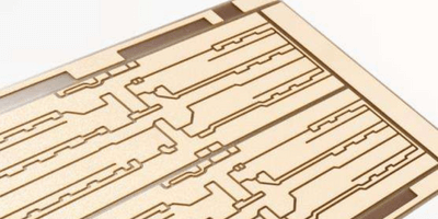
Home » PCB Manufacturing » Multilayer PCB
Compared with single-layer PCB and double-sided PCB, a multi-layer PCB is a printed circuit board with at least three conductive layers. The electrical connection between multilayer printed circuit board layers is realized through plated through holes on the circuit board. The number of layers of Multilayer circuit board can be 4, 6, 8, 10 Up to 100 layers.
More and more PCB manufacturers are involved in the multilayer PCB manufacturing industry, so the manufacturing process and technology have also developed rapidly. Fast turnaround multilayer PCB prototyping and assembly has become a reality.
A multilayer PCB might be better for your next project. Multilayer PCBs have more copper conductive layers and more wiring space, and the design of multilayer PCBs can achieve better signal transmission and electrical performance. The enormous advantages of multilayer PCBs enable more and more complex applications.
The manufacturing process of multilayer PCB is more complicated than single-layer or double-sided PCB, and the multilayer PCB manufacturing process requires more attention to detail. Multilayer PCBs achieve electrical connections between different layers through plated via holes, buried holes, or blind holes.
With JHYPCB’s extensive manufacturing capabilities and facilities for complex multilayer PCBs, you will get reliable, high-quality multilayer PCBs.

Multilayer PCBs Complete Guide
- What is Multilayer PCB?
- What are the benefits of multilayer PCBs?
- What Are The Multilayer PCB Applications?
- How many layers are there in multilayer PCB?
- Why Is There Any Need for Multilayer PCBs?
- Multilayer PCB Manufacturing Process
- Multilayer PCB Manufacturing Capabilities
- Multilayer PCB Manufacturer in China
- Multilayer PCB FAQs
What is Multilayer PCB?
The term multilayer represents the number of copper/conductive layers in a PCB. A single-layer PCB has only one conductive layer; however, it has other layers, such as the base layer, lamination, and insulating layer. A PCB is known or defined by the number of conductive/copper layers it inherits.
A multilayer PCB contains three or more copper layers. Thus, there can be 3, 4, 5…, 50…, 100, or even more layers. Keep in mind that it is not possible to place the components on all layers of a multilayer PCB, as they can only be placed over the surface layers. The other layers of PCB are used to distribute the connection and wiring between. The connections are distributed among the layers, which is why complex operations are possible, and connections can be made without wasting the space on the board.
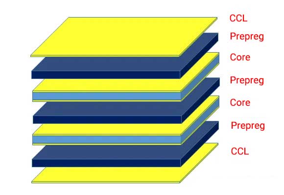
Multilayer PCB Stack up
What are the benefits of multilayer PCBs?
Multilayer PCBs provide improved performance and higher density, allowing greater functionality, capacity, and speeds.
- Smaller size – Reduced form factor
- Light-Weight
- High Durability
- Increased flexibility
- Higher assembly density
- Better controlled impedance features
- Better EMI Shielding
- Learn More
What Are The Multilayer PCB Applications?
Multilayer PCBs have become an integral part of electronic products and are widely used in many industries, including but not limited to:
- Computers
- Medical Equipment
- Satellite Systems
- Wearable Devices
- Defense
- Aerospace
- Telecommunication
- Electronics
- Learn More
How many layers are there in multilayer PCB?
Multilayer PCB is a PCB built up of more than two layers. It has at least three layers of conductive material within the insulating material.
- 4 Layers
- 6 layers
- 8 layers
- 10 layers
- 12 layers
- up to 100 layers
- Learn more about the multilayer PCB stack-up and thickness
Why Is There Any Need for Multilayer PCBs?
It is quite difficult, and most of the time impossible, to implement a complex design and obtain the product requirements from a single-layer or double-layer PCB. Single or double-layer PCBs are suitable for simple products, equipment, and devices, but when it comes to implementing complex designs, such as computer motherboards and smartphone PCBs, there are many constraints.
The first crystal-clear constraint is the space on the board. For complex designs, the single-layer and double-layer PCBs will take too much space, and consequently, the product will be bulky. We cannot make a compact product without using a multilayer PCB.
The most disturbing constraint in simple PCBs is the connection of the components. For connecting different components, there will be more space required, and it is important to use jumpers and wires. End-to-end wiring of complex designs is almost impossible in simple PCBs.
In a multilayer PCB, the presence of different layers offers a conductive route for the connection of components and passage of signals, which is why it has the potential to implement complicated designs.
Multilayer PCB Manufacturing Process
First, the PCB manufacturer’s engineering team will pre-review and evaluate the PCB design files provided by the customer, such as Gerber files, to obtain information for producing multilayer PCBs, such as the number of layers, board thickness, surface finish, solder mask, Materials and other information to match the factory’s process capabilities.
Second, multilayer PCBs are fabricated by laminating alternating prepreg (PP) and core materials together under high temperature and pressure. The lamination process ensures that air is not trapped between the layers and that the adhesive holding the layers together is adequately melted and cured.
There are many materials for multilayer PCB manufacturing; rigid multilayer PCBs are FR4, High Tg materials or high-frequency materials, and polyimide or polyester films for flexible PCB manufacturing.
Recommended reading:
Multilayer PCB Manufacturing Capabilities
JHYPCB has been manufacturing multilayer PCBs for 10 years. Over the years, we have fabricated all type of multilayer constructions from various industries and solved all types of problems with multilayer PCBs.
Multilayer PCB manufacturing is our primary business, and our strong PCB manufacturing capabilities can meet your multi-layer PCB manufacturing needs.
| Capability | Standard |
| Layers | Rigid Multilayer PCB up to 30 layers |
| Flexible Multilayer PCB up to 10 layers | |
| Multilayer Aluminum PCB up to 4 layers | |
| Materials | Rigid Material: FR4, Shengyi, Isola, High-Tg, High-frequency |
| Flexible Material: Dupont PI, Shengyi PI | |
| Thickness | Rigid Multilayer PCB: 0.1-8.0mm |
| Flexible Multilayer PCB: 0.05mm+/-0.02mm | |
| Surface Finish | Organic Solderability Preservative (OSP) |
| Hot Air Solder Level (HASL) | |
| Electroless Nickel / Immersion Gold/Silver/Tin | |
| Hard Gold (Gold Fingers) | |
| Carbon | |
| Peelable | |
| Custom Specified Surface Finishes are available! | |
| Solder Mask | Green, White, Blue, Black, Red, Yellow, etc. |
| PCB Inspection and Testing | Flying Probe test |
| Manual Visual Inspection | |
| Functional Testing | |
| Impedance Controlled Test | |
| Solderability Test | |
| Thermal Shock Test | |
| Automated Optical Inspection |
Multilayer PCB Example
Multilayer rigid PCBs are made of FR4 copper-clad laminates. They can be 4-layer, 6-layer, or even more copper layers.

Flexible PCB is a printed circuit made of insulating substrates such as PI. Flex PCB can be single-layer, double-sided or multi-layer flexible circuit boards.
A metal core PCB is a special PCB having a metallic base layer. This base layer is usually made of aluminum or copper. It is named MCPCB.
Due to its excellent heat dissipation characteristics, aluminum has been widely used as a thermally conductive material for printed circuit boards.
Ceramic PCB is better than fr4 PCB due to its heat dissipation performance, current carrying capacity, insulation, thermal expansion coefficient, etc.
Why Choose JHYPCB as your Multilayer PCB Manufacturer?
JHYPCB is a experienced multilayer PCB manufacturer in China
As a leading multilayer PCB manufacturer with more than 10 years of experience in the PCB manufacturing industry, you can expect products that meet the highest quality standards.
DFM Checks
Our detailed design for manufacturability checks begins with receipt of your Gerber files to catch errors (if any) early and save your cost.
State of the art technology
We have state-of-the-art manufacturing capabilities, utilizing the latest equipment, to ensure that our products are consistent with your requirements.
Short Lead Times
No matter the size of your order – our experienced team is committed to delivering to you on time with short lead times.
Prototype to High Volume
We provide multilayer PCB prototypes with a quick turnaround and mass multilayer PCB manufacturing services.
Multilayer PCB FAQs
Before designing a multilayer PCB, the designer needs first to determine the circuit board structure to be used according to the circuit scale, the circuit board size, and electromagnetic compatibility (EMC) requirements, that is, to decide whether to use 4 layers, 6 layers, or more layers of circuit boards. After determining the number of layers, determine where to place the internal electrical layers and distribute different signals on these layers. This is the choice of multilayer PCB stack structure. The laminated structure is an essential factor that affects the EMC performance of the PCB board, and it is also an essential means to suppress electromagnetic interference.
There are many factors to consider when determining the laminated structure of the multilayer PCB board. From the perspective of wiring, the more layers, the better the wiring, but the cost and difficulty of board manufacturing will also increase. For manufacturers, whether the laminated structure is symmetrical or not is the focus that needs to be paid attention to when manufacturing PCB boards. Hence, the choice of the number of layers needs to consider the needs of all aspects to achieve the best balance.
Printed circuit boards are divided into single-sided, double-sided, and multilayer PCBs, among which the number of layers of the multilayer PCB is not limited. There are already more than 100-layer PCBs, and typical multilayer PCBs are 4-layer boards and 6-layer boards.
The PCBs we often see are even-numbered layers, so why are PCB multilayer boards all even-numbered layers?
Because PCBs with even-numbered layers are indeed more advantageous than PCBs with odd-numbered layers.
1. Cost factors
The cost of raw materials used in producing odd-numbered PCBs is slightly lower than that of even-numbered PCBs. This is because odd-numbered PCBs lack a layer of dielectric and copper-clad laminate. However, the processing cost of odd-layer PCBs is significantly higher than that of even-layer PCBs.
2. The even-numbered PCB has a well-balanced structure to avoid warpage
The best reason not to design PCBs with odd layers is that odd-numbered circuit boards tend to warp. The substrate used for multilayer PCB manufacturing is double-sided, with copper on both sides. The factor that needs to be considered when designing or producing a multilayer PCB is that when the substrate has copper on one side and no copper on the other side, the thermal expansion coefficients of the two sides of the board are different after being heated. Due to the principle of thermal expansion and contraction, the board will warp after processing. Therefore, even if an odd-numbered PCB is required to achieve the required functions, we will design it as an even-numbered layer, design the 5-layer into 6-layer, and the 7-layer into 8-layer board.
In the multi-layer PCB design, one of the essential issues that need to be considered is how many circuit layers, ground layers, and power layers are needed to realize the functions required by the circuit. The stack-up design of a multi-layer PCB is usually decided after considering various factors.
So, what principles do you need to follow when designing a multi-layer PCB stack-up?
1. The distribution of layers
A multilayer PCB usually contains signal layer (S), power layer (P), and ground layer (GND). The power plane and the ground plane are usually entities without separation, which provide an excellent low-impedance current return path for the current of adjacent signal traces. The signal layer is usually located between these power or ground reference plane layers; the top and bottom layers of a multilayer PCB are usually used to place components and a small number of traces.
2. Single power plane
Decoupling capacitors can only be placed on the top and bottom layers of the PCB. The traces, pads, and vias of the decoupling capacitor will seriously affect the effect of the decoupling capacitor. This requires the design to consider the traces connecting the decoupling capacitors as short and wide as possible; the wires connected to the vias should also be as short as possible.
3. Multiple power layers
The multi-power plane will be divided into several physical areas with different voltages. If the signal layer is close to the multi-power supply layer, the signal current on the signal layer nearby will encounter an undesirable return path. Therefore, it is required that the high-speed digital signal wiring should be far away from the multi-power supply plane.
4. Multiple ground layer
Multiple ground planes can provide an excellent low-impedance current return path and can also reduce common-mode EMI. The ground plane and the power plane should be tightly coupled, and the signal layer should also be tightly coupled with the adjacent plane.
5. Reasonably design the wiring combination
The two layers spanned by a signal path are called a “wiring combination.” The best wiring combination design avoids the return current flowing from one reference plane to another but from one point on one reference plane to another.
Single-point and multi-point grounding methods:
- Single-point grounding: The ground wires of all circuits are connected to the same point on the ground plane, divided into series single-point grounding and parallel single-point grounding.
- Multi-point grounding: The ground wires of all circuits are grounded nearby, and the ground wires are short and suitable for high-frequency grounding.
- Mixed grounding: mix single-point grounding and multi-point grounding.
The more layers of PCB, the more difficult it is to manufacture, and the higher the manufacturing cost. The number of PCB layers is determined by the actual application requirements of the product. When designing a multi-layer PCB, the designer also needs to consider the feasibility of the process, production cost, function realization, and other factors to determine the number of layers of the PCB.
Multilayer flexible PCB can be divided into the following three types
1) A multilayer PCB is formed on a flexible insulating substrate, and the finished product is specified to be flexible. This structure is to bond the two side ends of many single-sided or double-sided microstrip flexible PCBs together. Still, the central parts are not bonded together, thus having a high degree of flexibility. To have the desired electrical characteristics, such as the characteristic impedance performance and the rigid PCB to which it is interconnected, each circuit layer of the multilayer flexible PCB component must be designed with signal lines on the ground plane. A thin, suitable coating, such as polyimide, can be used on the wiring layer instead of a thicker laminated cover layer to have a high degree of flexibility. This multilayer flexible PCB is most suitable for designs that require flexibility, high reliability, and high density.
2) A multilayer PCB is manufactured on a flexible insulating substrate, and the finished product can be flexed. This type of multilayer flexible PCB is made of flexible insulating materials, such as polyimide film, laminated to make a multilayer board, which loses its inherent flexibility after lamination. This type of flexible PCB is used when the design requires maximum use of the insulating properties of the film, such as the low dielectric constant, uniform thickness of the medium, lighter weight, and continuous processing. For example, a multilayer PCB made of polyimide film insulating material is about one-third lighter than a rigid PCB with epoxy glass cloth.
3) Multi-layer PCBs are made on a flexible insulating substrate, and the finished product must be shapeable, not continuously flexible. This type of multilayer flexible PCB is made of flexible insulating materials. Although it is made of flexible materials, due to electrical design restrictions, such as the required conductor resistance, a thick conductor is required, or for the required impedance or capacitance, a thick conductor is required between the signal layer and the ground layer. It is insulated and isolated, so it is already formed in the finished application. The term “formable” is defined as a multilayer flexible PCB component that can be shaped into the required shape and cannot be flexed in the application—used in the internal wiring of avionics units. At this time, it is required that the conductor resistance of the stripline or three-dimensional space design is low, the capacitive coupling or circuit noise is minimal, and the interconnection end can be smoothly bent to 90°. Multilayer flexible PCB made of polyimide film material achieves this wiring task. Because the polyimide film is resistant to high temperatures, flexible, and has good overall electrical and mechanical properties. To achieve all the interconnections of this component section, the wiring part can be further divided into a plurality of multilayer flexible circuit components combined with adhesive tape to form a printed circuit bundle.
1. Alignment between layers
Since there are more layers in a multilayer circuit board, the requirements for alignment between layers are also higher. Generally, the alignment tolerance between the layers is controlled at 75 microns. Due to the influence of factors such as size and temperature, the degree of difficulty in controlling the alignment between layers of a multilayer board will be huge.
2. Inner circuit production
Multilayer circuit boards use unique materials such as high TG, high speed, high frequency, thick copper, the thin dielectric layer, etc. This puts forward high requirements for inner circuit production and pattern size control. For example, the integrity of impedance signal transmission increases the difficulty of internal circuit manufacturing. The line width and line spacing are small, the probability of open circuit and short circuit may increase; the increase of short circuit will reduce the pass rate; the number of thin lines signal layers will increase the probability of missing AOI detection in the inner layer; the inner core board is light and easy to wrinkle, Poor exposure and easy curling during etching; the unit size of multilayer PCB is more significant, and its product scrap cost is higher.
3. Pressing process
Many inner core materials and semi-cured boards are superimposed, and defects such as slippage, delamination, resin voids, and bubble residues are prone to stamping production. In the design of the laminated structure, the heat resistance, pressure resistance, glue content, and dielectric thickness of the material should be fully considered, and a reasonable material pressing plan for the multilayer circuit board should be formulated. Due to many layers, the expansion and contraction control and the dimensional coefficient compensation cannot maintain consistency, and the thin interlayer insulation layer is likely to cause the interlayer reliability test to fail.
4. Drilling
The use of high-TG, high-speed, high-frequency, and thick copper special plates increases the difficulty of multi-layer PCB drilling roughness, drilling burrs, and decontamination. Due to a large number of layers, the copper thickness and plate thickness have also increased, and tool breakage is likely to occur during drilling; if there are many BGAs, the narrow hole wall spacing can easily lead to CAF failure; the increase in plate thickness can also easily lead to the problem of diagonal drilling.
The meaning of the different layers of a multi-layer PCB
a. Signal Layers: Signal layers include Top Layer, Bottom Layer, Mid Layer 1……30. These layers are all layers with electrical connections, that is, the actual copper layer. The middle layer refers to the middle board layer used for wiring, and the wires are distributed in this layer.
b. Internal Plane: Internal Plane or inner layer 1……16. These layers are generally connected to the ground and the power source and become the power layer and the ground layer. They also have electrical connections and are also the actual copper layer. Generally, there is no wiring, and it is composed of a whole piece of the copper film.
c. Silkscreen Overlay: The top silkscreen layer (Top overlay) and the bottom silkscreen layer (Bottom overlay). The silkscreen characters that define the top and bottom layers are generally text symbols printed on the solder mask, such as component names, component symbols, component pins, copyrights, etc., to facilitate future circuit soldering and error checking.
d. Paste Mask: Including the top paste layer and the bottom paste layer (Bottom paste), which refers to the exposed surface-mount pads that we can see, that is, before soldering the part that needs to be coated with solder paste. Therefore, this layer is also helpful for hot air leveling of the pads and producing the welded stencil.
e. Solder Mask: It includes the top solder mask and the bottom solder mask. Its function is opposite to that of the solder paste layer. It refers to the layer to be covered with green oil. This layer is non-sticky solder, preventing the excess solder of adjacent soldering points from short-circuiting during soldering. The solder mask covers the copper film wires, and the copper film is too quickly oxidized in the air but leaves a place at the solder joints and does not cover the solder joints.
f. Mechanical Layers: Up to 16 mechanically processed layers can be selected. Designing a double-sided PCB only needs to use the default option Mechanical Layer 1.
g. Keep Out Layer: Define the boundary of the circuit layer. After defining the keep-out layer, the wiring with electrical characteristics must not exceed the boundary of the keep-out layer in the subsequent wiring process.
h.Drill Layer: including drill guide and Drill drawing.
I. Multi-layer: Refers to all layers of the multilayer PCB.
The thickness of the PCB board is mainly determined by factors such as copper thickness, material, number of layers, and application requirements. The standard board thickness of the PCB is about 62 mils (that is, what we usually call 1.60 mm PCB). With the needs of the application, the copper thickness and the number of layers of the PCB are constantly increasing. Therefore, the PCB is often thicker than before. According to customers’ designs and requirements, multilayer PCB manufacturers can provide customers with various options. (For example, 93 mil or 2.36 mm, and 125 mils or 3.17 mm; this is 150% and 200% of the old standard thickness).
The cost of a multilayer PCB correlates with the number of layers — the more layers, the higher the price. Also, some multilayer PCBs may require more manufacturing time, which can impact the cost of a project.
Ultimately, the cost of a multilayer PCB comes down to a few things:
- The number of layers
- Level of complexity
- Quantity
How to order multilayer PCBs?
For a fast and accurate multi-layer PCB quote, when ordering a multi-layer PCB from a PCB manufacturer, be sure to provide accurate information such as material selection, lamination sequence, board thickness, tolerance requirements, processing techniques, etc. When exporting the PCB to Gerber, it is recommended to use the RS274X format. The RS274X format has the following advantages: the CAM system can automatically input data, and the whole process does not require manual participation, which can avoid many troubles, and can maintain good consistency and reduce the error rate.
Get Your Multilayer PCB Today!
JHYPCB is one of the leading PCB manufacturers in China, fully equipped with state-of-the-art machinery and the latest technology. We offer high-quality multilayer PCBs of up to 30 layers without any restriction on the number of pieces; you can order one PCB or PCBA. Our experts understand the complexity of multilayer PCB and ensure high-performing PCBs and PCBA.
JHYPCB is RoHS, UL, and ISO compliant and certified. We ensure optimum quality in the minimal delivery time. Customers can get turnkey and quick prototype and assembling services. For more information and details, feel free to contact us.