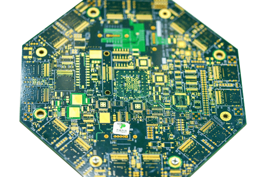
In the production of multilayer PCB, the quality of engineering data plays a pivotal role. It contains all the data needed in the entire production and involves various processes of the multilayer PCB production.
Any small error in the engineering data may bring significant losses to the production. A simple processing technique of engineering data will significantly facilitate the production of multilayer PCB boards. Therefore, measures such as improving the requirements for the production of engineering data, standardizing the primary content and methods of engineering data processing, strengthening the systematic inspection of engineering data, and strengthening the rationalization of the engineering data production process are essential. These measures improve the production quality of engineering data.
1. Requirements for Engineering Data in the Production of Multilayer PCB
The engineering data of the multilayer Circuit board must be based on the complete realization of the designer’s requirements. It must provide maximum convenience for production so that the multilayer printed circuit board manufacturer can quickly and safely realize the design requirements. Therefore, the designer’s requirements for printed circuit boards are the ultimate goal of engineering data production. The production of engineering data should make full use of existing equipment resources, processing methods, and processing capabilities to achieve the technical requirements proposed by the designer.
2. Production Process of Multilayer PCB Engineering Data
The production of engineering data is carried out on the CAD/CAM system. First, review the design content data of the PCB file (including the highest number of layers, board thickness, minimum line width, and line spacing, minimum finished aperture, board outline dimensions, tolerance, aperture tolerance, special requirements, etc.) and Gerber format data confirmed by the CAM system conversion.
Secondly, under the premise of ensuring PCB design requirements according to the production capacity and process capability of the production line and from the perspective of processability, check and modify the Gerber files of each layer of the printed circuit board and perform DRC checks on the Gerber files. Finally, the PCB graphics unit performs automatic PCB board assembly and CAM outputs optimized light drawing data, drilling, and milling data, flying probe detection data, copper area for electroplating, and preparation of manufacturing instructions.

3. Requirements for the Production of Engineering Data for Multilayer Printed Circuit Boards
The engineering data for multilayer printed circuit board production are the guiding process documents for printed circuit board production. It aims to achieve the design requirements, and it must meet the production line capacity to the greatest extent.
3. 1 Requirement for the Production of Shapes and panelize
The production of the shape data is to make the milling shape file according to the PCB outline drawing provided by the designer. The outline production rules are as follows.
(1) If there is no requirement for the design, the data shall be subject to the actual measurement of the document. If the data provided by the designer or the design document has a unique data mark, check whether the data is contradictory and whether the tolerance exceeds the capacity range.
(2) Shape positioning requires 3 NPTH holes for positioning. The shape positioning holes in the shape data should correspond to the positioning holes on the board, and the positioning holes are not in a straight line.
(3) Try to use large milling cutters when milling the shape to reduce tool breakage and improve the efficiency of shape processing.
(4) For the bridge plates, pay attention to the torque generated by the splicing plate connection method. It may cause a situation that they cannot be broken entirely after production.
(5) The profile data should include a description file for profile processing, including the milling profile file name, milling cutter size, positioning hole tool size, and drilling positioning hole file name.
After the shape is determined, the printed circuit board unit is assembled to ensure the minimum size of the printed board allowed by each device and improve the production efficiency of the printed circuit board.
The panelize rules are as follows.
(1) Pay attention to the spacing of graphic units to leave enough milling cutter space for the milling shape. The board’s edge should be as slight as possible, but it should meet the requirements for the side of the board in processes such as electroplating and lamination.
(2) Improve the distribution of lines, help disperse current in electroplating, and reduce over-corrosion by etching.
(3) High-level digital boards, dense-line boards, and other boards with high alignment accuracy requirements are not suitable for massive commissions.
(4) To reduce the warpage, hot-air screed plates with a plate thickness of ≤1.2 mm are not suitable for large platters.
(5) The gold finger of the gold fingerboard joins the board in the direction outside the board.
(6) Cutting size design: length and width cannot be equal.

3. 2 Production Requirements for Drilling Data
If the design has no special instructions, the plan provides the finished hole diameter and its tolerance. The drilling hole position, hole number, and PTH/NPTH hole must be marked. Make drilling files according to the hole position in the PCB graphics and the design requirements for the hole size.
(1) Check massive holes and overlapping holes. If the hole diameter is the same, delete it to only one spot. If the hole diameter is inconsistent, confirm the hole diameter; overlapping holes will lead to undesirable phenomena, such as drilling holes, knife breaking, hot air leveling, and blasting (except stamp holes). Please ask the designer whether to drill between two shafts or drill two holes into slots.
(2) Before generating the drilling file, the aperture tolerance requirements and the copper plating process must be used for aperture compensation in the CAM system.
(3) Compare the drilling data with the shape data and check whether there are broken holes caused by the intersection with the shape, whether the positioning holes and the holes of the drill shape are added to the drilling data. Compare the drilling data with the line graphics of each layer; check whether the drilling may affect the electrical connection of the circuit, such as whether the hole is drilled to break the wire or cause a short circuit.
(4) The distance of drilling positioning holes on the side of the multilayer PCB board must be equal.
(5) Use the drilling data of the PCB file as the basis to check the drilling data for production. Check the type and quantity of drilling, whether there are too many and leaks. In addition to the drilling file, the drilling data also includes a list of drill rows corresponding to the drilling file. The main content consists of the size of the drill and the number of holes.
3. 3 Negative Film Production Requirements
3. 3. 1 Requirement for Production of Circuit Layer Negatives
The circuit layer negatives include inner and outer circuit negatives. You must follow the following rules.
(1) For the designed non-plated through-holes or process holes added outside the PCB pattern, ensure an isolation area between the inner and outer circuit patterns.
(2) Check the width of the solder ring and make appropriate compensation for the small solder ring pad. If it appears that the pad cannot be enlarged to ensure the distance between the disks, you can communicate with the designer to add a teardrop pad or change an oblong pillow or delete it. It would be best to have appropriate compensation for wire width and wire spacing according to the selected copper thickness.
(3) The subtle seams that are likely to cause open circuits on the dry film should be added. The grids of the outer circuit patterns that are likely to cause solder mask bubbles should be treated to reduce the unevenness of the coating. If there is an uneven distribution of the outer circuit, then the graphics need to be modified.
(4) Open the power layer, ground layer, and dot map simultaneously, check that there is at least one isolation disk on each hole; otherwise, the power layer and ground layer will be short-circuited. Generate the network of the light drawing files of each segment and light up the grounded copper skin. The copper skin connected to the power supply should not be bright; otherwise, it will be short-circuited. Conventionally, two-pin devices will not appear on the same network with two pins.
(5) If there is a large area of copper on one side, then to avoid warping, the PCB file should be modified into two teams of copper or grid.
(6) There is a narrow area between the isolation bands of the design file, or the isolation disks are dense. Check whether it will cause an open circuit after the isolation disk or thermal pad compensation.
(7) Check whether the endpoint of the printed wire of the design file is connected to the pad to prevent an open circuit caused by the shrinking of the pad when the project is modifying it.
(8) The line graphics of each layer that is too close to the outline must be moved.
(9) Add a baffle block to the broad base material area of the contour groove or the inner groove. If the designed wiring is not uniform, it is recommended to add a baffle block in the base material area to prevent white spots, warping, and other undesirable phenomena.
(10) For uniform electroplating, it is necessary to add auxiliary electroplating blocks to the edges of each panel, panel gaps, and internal cell grooves. Be careful not to expose the copper.
(11) If there is an isolated reflective point without a copper ring, it is recommended to add a copper ring to avoid dots falling after etching.
3. 3. 2 Production Requirements for Solder Mask and Character Negative
(1) Based on the solder mask pattern provided by the designer, make the solder mask pattern according to the land size in the processed circuit pattern. The size of the solder mask pattern should be larger than the corresponding circuit pattern to ensure that the solder mask cannot be placed on the land.
(2) When the distance between SMT pads is small, and the design requires solder resists between SMT pads, the solder resists pattern of SMT pads should be lower.
(3) The holes drilled on the printed circuit board and the added process holes should be combined with a solder mask pattern more significant than the drill diameter to prevent the solder mask ink from entering the hole and causing the aperture size to be too small.
(4) Make drilling files for the BGA via solder mask and perform solder mask plug holes.
(5) When the edge of the solder mask is too close to the printed line, the solder mask can be reduced or cut. If it is too close to the copper skin, the copper skin can be cut while ensuring the electrical performance of the printed circuit board.
(6) Check whether the character crosses the solder mask pattern and deal with the cross part to prevent the character from being placed on the plate or entering the hole.
(7) If the characters are on a large tin surface, the characters do not need to be cut, and the characters are required to be flattened by hot air before silk-screen printing.
4. Suggestions for the Production of Engineering Data
Sometimes it is required to make manufacturability modifications to the designed PCB file. Since designers are not necessarily very familiar with the manufacturing of printed circuit boards, they rarely consider the difficulties of printed circuit boards when designing. Some manufacturing problems can be avoided only by modifying the PCB graphic design according to the multilayer PCB manufacturing process without changing the electrical performance of the printed circuit board.
Pay attention to investigating the requirements of engineering data in the production process. Engineering data must be able to facilitate production. Only after production inspection can it be known whether the engineering data are convenient for production. Besides, some processing methods conducive to production must be timely applied to the creation of engineering data, which improves the usability of engineering data.
Conclusion
In short, whether the engineering data meets the process, production capacity, and processability of the production line under the premise of ensuring the design requirements of the multilayer PCB board is an essential aspect of engineering production. Therefore, engineers must have a considerable degree of familiarity with the processing capacity and corporate standards of each process of the production line. They should have a certain degree of understanding of the operation processes. When making engineering changes, understand the entire process production to make correct changes and ensure that the changes are complete. The different design requirements of the printed circuit board, the production line process, the production capacity, and the specific production requirements of the engineering data is also different. The particular parameters based on the production and inspection process are continuously accumulated during the FR4 multilayer PCB production process.
Advanced Learning:
- What is a Multilayer PCB and What are the Advantages?
- Rigid PCB Circuit Board Fabrication Services
- Plated Through Hole, Blind Via, and Buried Via in PCB Fabrication
- Angle Control in Multilayer PCB
- 6 Layer PCB Board-Stackup, Thickness, Fabrication, And Price
- The Most Important Things You Need To Know About Single-layer PCB
- Low-cost Double-sided PCB Board Prototype Production service
- A Free Software for PCB Design for Manufacturing or DFM Analysis


