What is Via Hole in PCB?
Via is one of the important components of multilayer PCBs. This kind of hole connects the copper foil circuit in different circuit board layers.
In the PCB production process, drilling is essential. The simple understanding of drilling is to drill the required vias on the copper-clad board, which provides electrical connections and fixing devices. If the operation is incorrect, the process of via holes will be problematic. The device cannot be set on the circuit board, which will affect the circuit board’s use, and in the worst case, the entire panel will be scrapped. Therefore, the drilling process is essential.
The printed circuit board is formed by stacking many layers of copper foil. These copper foil layers cannot communicate with each other because each layer of copper foil is covered with an insulating layer, so they need to rely on Vias for signal connection.
PCB Via Hole Classification
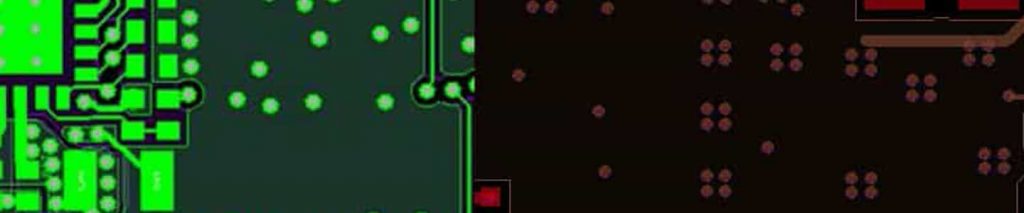
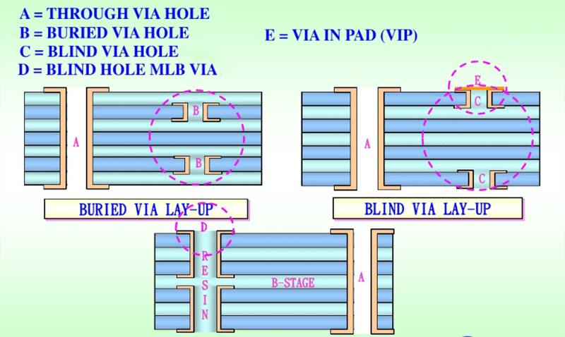
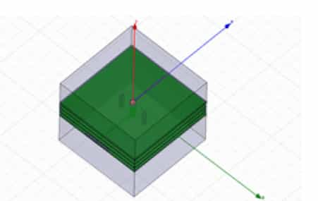
Simply put, every hole on the PCB can be called a via. Regarding function, vias can be divided into two categories: one for electrical connection between layers, and the other for fixing or positioning devices. In terms of process, these vias are generally divided into three categories, namely blind vias, buried vias, and plated through-hole.
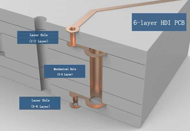
Blind via holes are located on the top and bottom surfaces of the printed circuit board and have a certain depth. They are used to connect the surface circuit and the underlying inner circuit. The hole depth usually does not exceed a certain ratio (aperture).
The buried via hole refers to the connection hole located in the inner layer of the printed circuit board, which does not extend to the surface of the circuit board. The above-mentioned two types of holes are located in the inner layer of the circuit board and are completed by a through-hole forming process before lamination, and several inner layers may be overlapped during the formation of the via.
The third type is called a plated through-hole, which penetrates the entire circuit board and can be used for internal interconnection or as a component mounting positioning hole. Because the through-hole is easier to implement in the process and the cost is lower, most printed circuit boards use it instead of the other two types of through-holes.
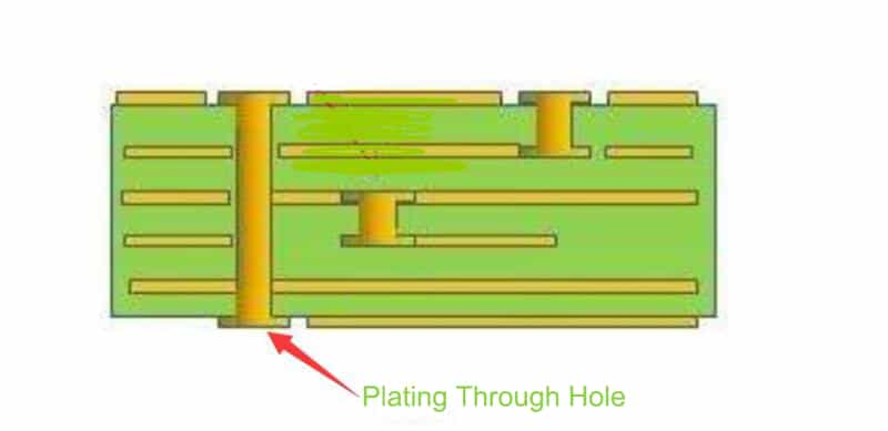
Plated Through Hole
Plated Through Hole is abbreviated as PTH. This is the most common type. If you pick up the PCB and face the light, the hole that can see the bright light is the “through hole.” This is also the simplest type of hole because you only need to use a drill or laser to drill the circuit board directly, and the cost is relatively cheap.
PCB Plated Through Hole Design
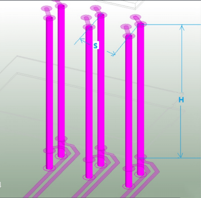
From a design perspective, a through-hole is mainly composed of two parts, one is the drill hole in the middle, and the other is the pad area around the drill hole. The size of these two parts is obvious. In the high-speed and high-density PCB design, PCB designers always hope that the smaller the via hole is the better. If there are smaller holes, more circuit routing space will be left on the circuit board. In addition, the smaller the via hole, the greater will be its own parasitic capacitance.
Small holes are more suitable for high-speed circuits. However, the reduction of hole size also brings an increase in cost. Moreover, the size of the vias cannot be reduced indefinitely. Process technologies, such as drilling and plating restrict it.

Small holes require more time for drilling. The longer the drill hole takes, the easier it is to deviate from the center position. Furthermore, when the depth of the hole exceeds 6 times the diameter of the drilled hole, it cannot be guaranteed that the hole wall can be uniformly plated with copper. For example, the thickness (through-hole depth) of a normal 6-layer PCB board is about 50 mil, so the minimum drilling diameter PCB manufacturers can provide is 8 mil.
Classification of Through Holes
Through holes are traditionally divided into plated (supported) through holes and non-plated (unsupported) through holes. “Supported” refers to the plating on the hole wall. Unplated or unsupported holes may or may not have pads, such as mounting holes and non-porous wall plating. This is a manufacturing term, but holes should be divided into two types: welded and unwelded for design.
Through Hole Aperture Size Calculation
In the through-hole aperture size, the inner diameter is ≥ 8mil (0.2mm); this is the minimum hole diameter for mechanical drilling. If it is a blind hole or buried hole, the minimum hole diameter is 4mil (0.1mm), and the laser makes this type of hole. The smaller the hole, the more expensive the PCB board will be. It is recommended to use 10/18, 12/20 holes for through holes, and 16/24 for power holes.
There is no absolute standard for PCB. The outer diameter can be made larger for high current, and the hole can be made smaller. However, PCB manufacturers generally recommend using 0.5mm inner diameter because they are not easy to break.
Blind Via Hole (BVH)
Blind Via Hole connects the outermost circuit in the printed circuit board with the adjacent inner layer with electroplated holes. One side of the hole can be seen because it is not the surface, but the other side of the hole cannot be seen, so it is called blind via hole. To increase the space utilization rate between the circuit layers of the circuit board, blind holes come in handy.
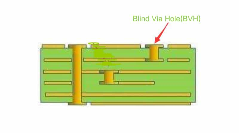
Blind holes are located on the circuit board’s top and bottom surfaces and have a certain depth. They are used to connect the surface line with the underlying inner line.
The depth of the hole generally has a specified ratio (aperture). This production method requires special attention, and the drilling depth must be just right. If you don’t pay attention, it will cause difficulties in electroplating in the hole. Therefore, few factories will adopt this production method. In fact, it is possible to drill holes for the circuit layers that need to be connected in advance in the individual circuit layers and then glue them together. Still, more precise positioning and alignment devices are required.
Buried Via Hole (BVH)
Buried Via Hole (BVH) connects any circuit layers inside the printed circuit board, but there is no conduction with the outer layer. There is no conduction extending to the surface of the circuit board. Drilling after the circuit board is bonded cannot achieve this production process. It must be drilled at the time of individual circuit layers. First, partial bonding of the inner layers is carried out, then electroplating, and finally, all layers are bonded. Since the operation process is more laborious than the original vias and blind holes, the price is also very high. This manufacturing process is only used for high-density circuit boards to increase the space utilization of other circuit layers.
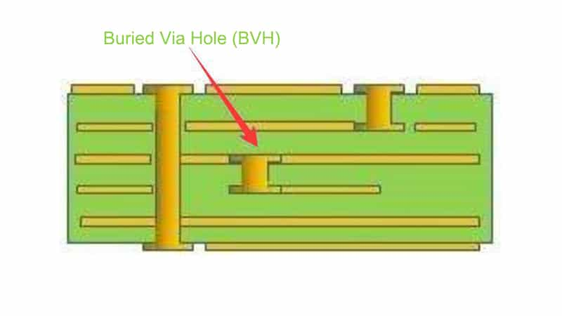
A buried hole means that the hole cannot be seen from the board’s appearance, but the actual hole is buried in the inner layer of the circuit board.
PCB Blind Hole and Buried Hole Specifications
The line width and line spacing of most process equipment are:
Blind Hole: 0.1mm, 0.125mm, 0.15mm.
Buried Hole: 0.15mm, 0.2mm, 0.25mm
Some PCB manufacturers can achieve a 4 mil line width and diameter and small apertures of 0.2mm and 0.1mm. The specifications are according to the requirements during PCB design and the manufacturing plant’s equipment process capability.
If it is a laser hole, it can be made relatively smaller. The minimum aperture can be 4mil (0.1mm). Generally, it depends on the design requirements of the hole. For example, the outer diameter should be larger for high current, and the hole can be small.
With the renewal and upgrade of our production equipment, the PCB process capability has been dramatically improved. Now the minimum aperture can be 0.1mm, the line width and line spacing can be 3mil (0.0762mm). The smallest laser hole can be 0.1mm, and the smallest mechanical hole can be 0.15mm.
Application of Non-through Via Technology
In non-through via technology, applying blind vias and buried vias can significantly reduce PCB’s size and quality, reduce the number of layers, improve electromagnetic compatibility, increase electronic product features, and reduce costs. It will also make the design work easier and faster.
In traditional PCB design and processing, through holes will bring many problems.
Firstly, they occupy a large amount of valuable space.
Secondly, many through-holes are densely packed in one place, creating a massive obstacle to the inner layer circuit wiring of the multilayer PCB. These through-holes occupy the space required for circuit wiring, and they densely pass through the power supply and the ground. The surface of the circuit wiring layer will also destroy the impedance characteristics of the power and ground wire layer and make them ineffective. And the conventional mechanical method of drilling will be 20 times the workload of using non-through hole technology.
Due to the non-through via technology, there are few large vias on the PCB that can provide more space for routing. The remaining space can be used for large-area shielding purposes to improve EMI/RFI performance. Simultaneously, more remaining space can also be used for the inner layer to partially shield the device and necessary network cables to have the best electrical account. The use of non-through vias makes it easier to fan out the device pins, making it easy to route high-density pin devices (such as BGA package devices), shortening the wiring length, and meeting the timing requirements of high-speed circuits.
Advanced Learning:


