- Home
- PCB Prototype
-
-
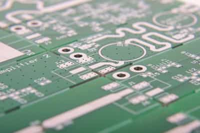
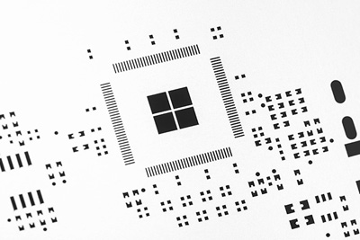
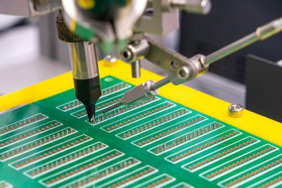
PCB Prototype Service
JHYPCB is a reliable PCB manufacturer in China and offers rapid PCB prototype service for quick-turn PCB fabrication at high quality and low cost. We can prototype your PCB within 3-7 days.
-
-
- PCB Manufacturing
-
-
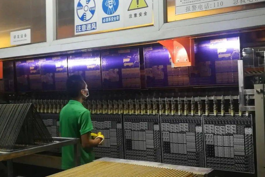
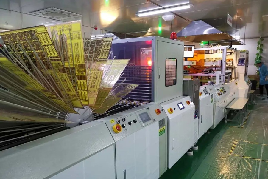
PCB Manufacturing Services
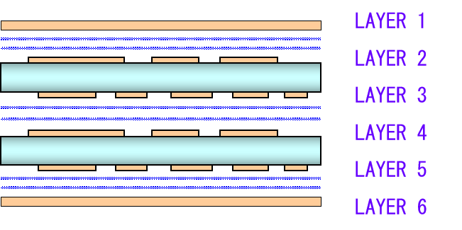
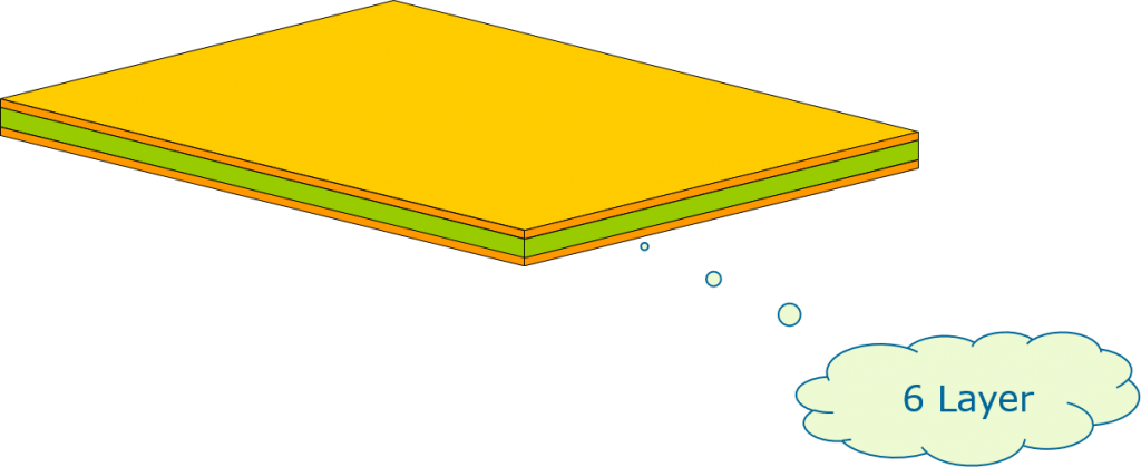
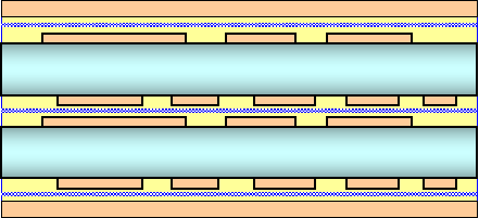
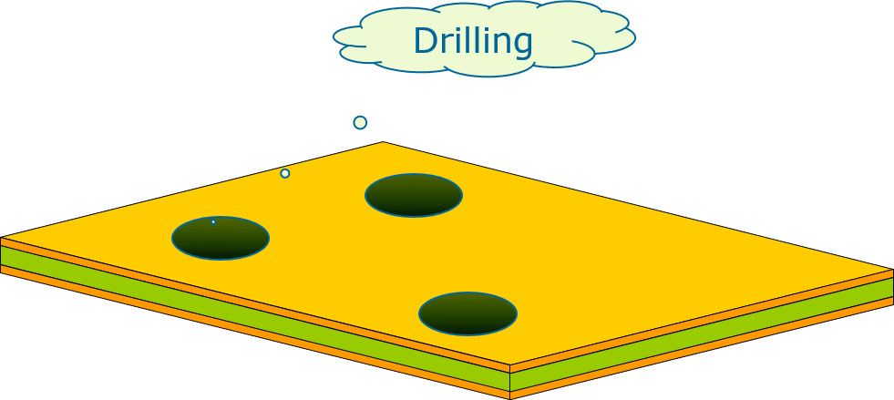
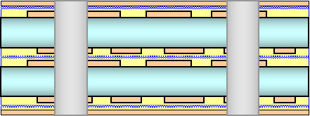
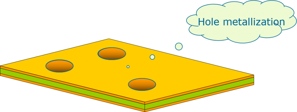
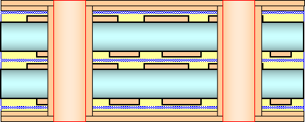
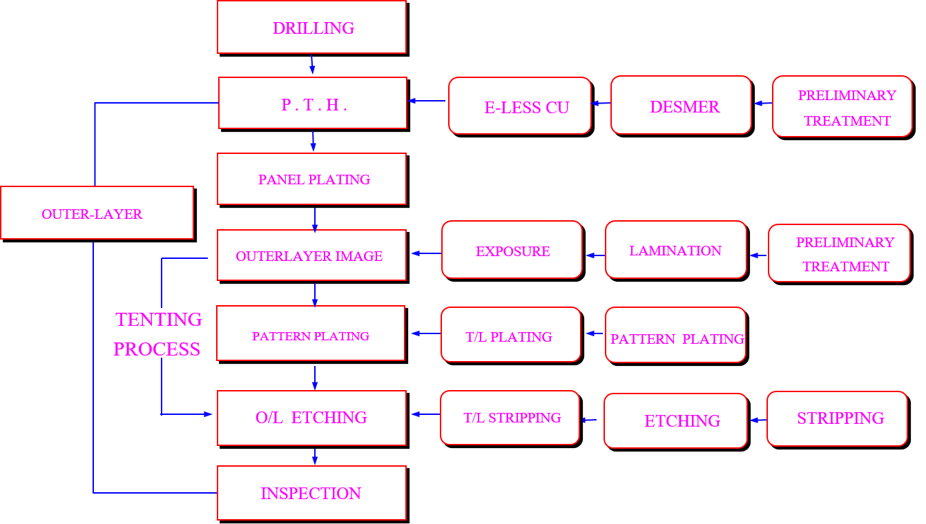
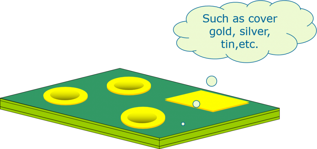
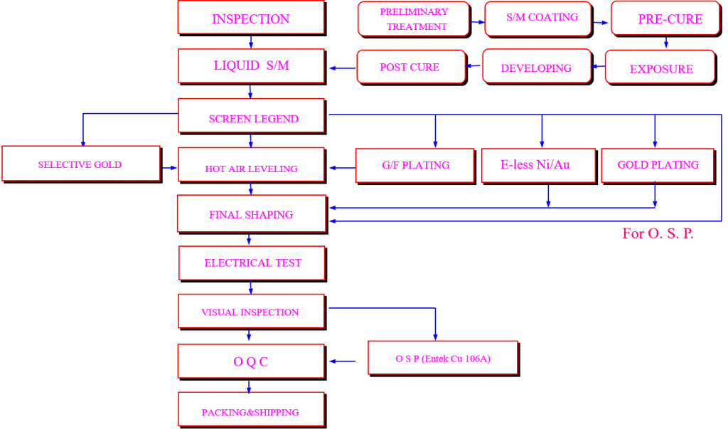
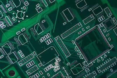
JHYPCB offers full feature PCB manufacturing services with high reliability to be compatible with your requirement. PCB fabrication services include rigid FR4 PCB, Flexible PCB, Rigid-flex PCB, HDI PCB, High-Frequency PCB, Rogers PCB, Multilayer PCB, Heavy Copper PCB, etc.
-
-
-
- PCB Assembly
-
-
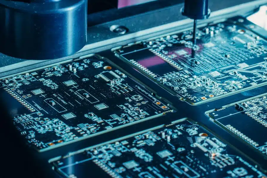
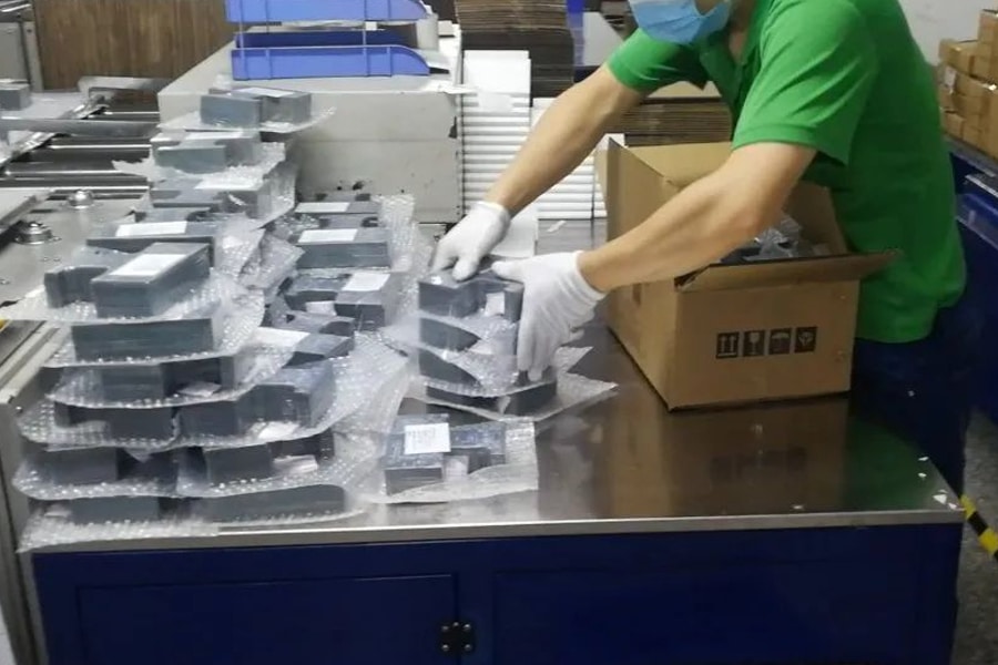
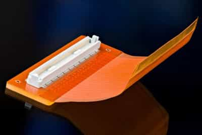
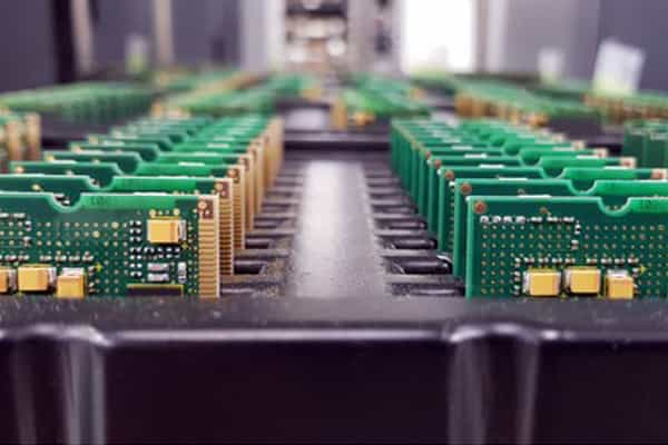
PCB Assembly Services
Full turnkey PCB assembly services in China. JHYPCB specializes in prototype PCB assembly, quick turn PCB assembly, and low-to-high volume PCB assembly services with production capabilities.
-
-
- About us
-
-
PCB Manufacturer in China
We are a leading PCB manufacturing & PCB assembly manufacturer and supplier in China. We have over ten years of experience in custom PCB fabrication and assembly with advanced PCB technology, high-quality standards & RoHS compliance.
-
-
-
- Industries Served
- PCBs For Consumer electronics
- PCBs For New Energy Applications
- New Energy Vehicle PCB
- PCBs for Automobile Electronics
- PCBs for Medical Devices
- PCBs for Industrial Control Applications
- PCBs for Communication Equipment
- Server and data storage PCBs
- Security and Access Control Systems PCBs
- PCBs for Aerospace and Defense
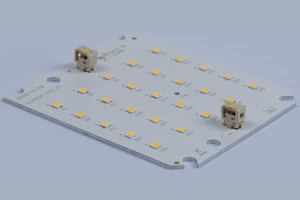
- PCBs for LED Lighting
- Industries Served
-
-
- Resources
-
-
Help Resources
A full-service electronic manufacturing company headquartered in China specializes in printed circuit board manufacturing and assembly services. We will provide a full range of technical support and services for the smooth progress of your project.
-
-
-
sales@pcbjhy.comsales@pcbjhy.com