Table of Contents
In today’s fast-paced world of electronics, surface mount technology (SMT) assembly has become an indispensable process in the manufacturing of modern devices. From smartphones and laptops to medical equipment and aerospace components, SMT enables the creation of compact, high-performance, and reliable electronic products.
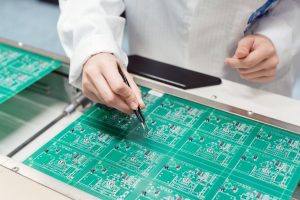
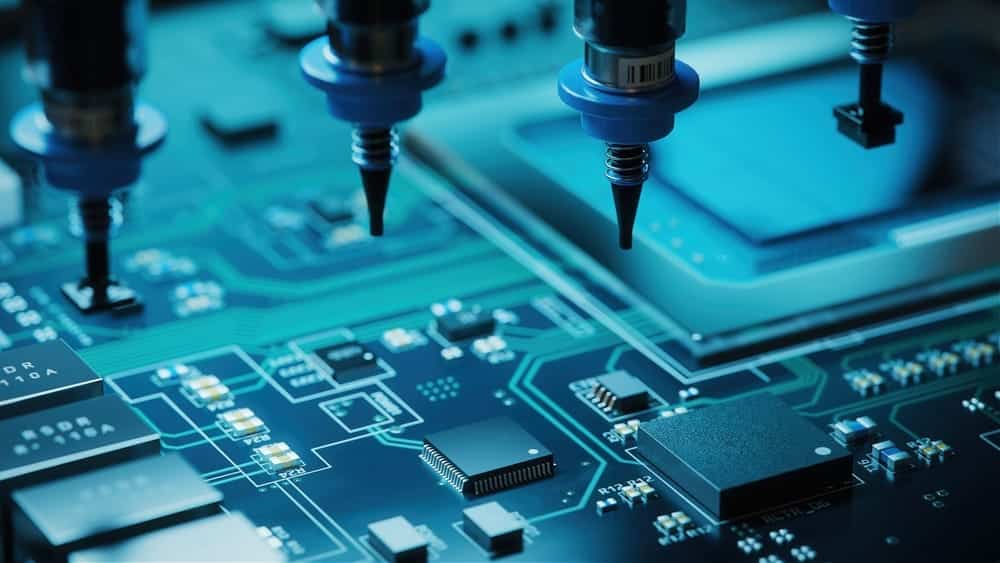
SMT assembly is a specialized process that involves mounting electronic components directly onto the surface of a printed circuit board. Unlike the traditional through-hole technology, where component leads are inserted into holes in the PCB, SMT components are soldered onto the surface, allowing for smaller component sizes and higher circuit densities.
The importance of SMT assembly cannot be overstated in today’s electronics industry. As consumer demand for smaller, lighter, and more powerful devices continues to grow, SMT assembly techniques have evolved to meet these requirements. With the ability to accommodate miniaturized components and intricate designs, SMT has revolutionized electronics manufacturing, enabling the creation of cutting-edge products that were once thought impossible.
In this comprehensive guide, we will explore the world of SMT assembly, delving into its processes, components, equipment, and applications. Whether you are a hobbyist, an engineer, or a manufacturer, this article will provide you with valuable insights into this crucial technology that drives the electronics industry forward.
What is SMT Assembly?
SMT assembly is a highly efficient and widely adopted method of manufacturing electronic circuits. It involves mounting electronic components directly onto the surface of a PCB using specialized soldering techniques. This process contrasts with the traditional through-hole technology, where component leads are inserted into holes drilled in the PCB.
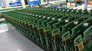
The key advantage of SMT assembly lies in its ability to accommodate smaller component sizes and higher component densities on PCBs. SMT components, often referred to as surface mount devices (SMDs), have miniaturized package styles with terminations or leads that are designed to be soldered onto the surface of the PCB. This miniaturization enables the creation of more compact and lightweight electronic products while improving performance and reliability.
Compared to through-hole technology, SMT assembly offers several significant advantages:
- Miniaturization: SMT components are significantly smaller than their through-hole counterparts, allowing for higher circuit densities and smaller product sizes.
- Cost-effectiveness: Automated SMT assembly processes are highly efficient, reducing labor costs and increasing production throughput.
- Improved reliability: SMT components have shorter lead lengths and are directly soldered to the PCB, resulting in stronger mechanical bonds and better resistance to vibration and shock.
- Enhanced electrical performance: Shorter lead lengths in SMT components reduce inductance and capacitance, improving signal integrity and high-frequency performance.
While SMT assembly has numerous benefits, it also presents challenges in terms of handling small components, precise placement accuracy, and specialized soldering techniques. However, with advanced equipment and stringent quality control processes, these challenges can be effectively addressed, making SMT assembly the preferred choice for a wide range of electronic products.
SMT vs SMD
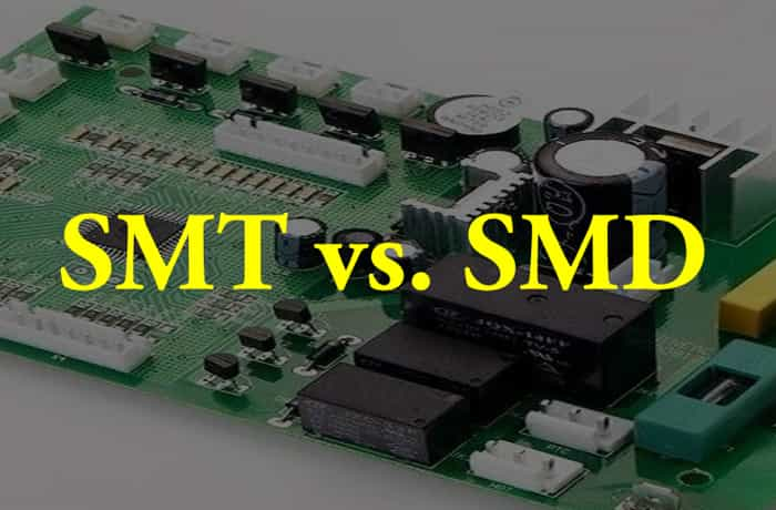
The terms “SMT” and “SMD” are often used interchangeably, but they refer to slightly different aspects of the surface mount assembly process.
SMT refers to the technology and manufacturing process of assembling electronic components directly onto the surface of a PCB using specialized soldering techniques. It encompasses the entire assembly process, including solder paste printing, component placement, reflow soldering, and inspection.
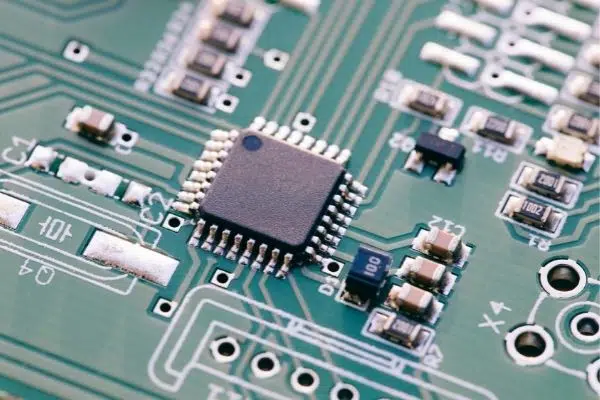
On the other hand, SMD, or Surface Mount Device, refers specifically to the electronic components themselves that are designed for surface mount assembly. These components have terminations or leads that are intended to be soldered onto the surface of the PCB, rather than being inserted into holes as in through-hole technology.
SMDs come in various package styles, such as:
- Chip components (resistors, capacitors, inductors)
- Flat packages (QFP, QFN, LGA)
- Ball grid arrays (BGA)
- Small outline packages (SOIC, SSOP)
These surface mount components are characterized by their compact size, high lead count, and close lead spacing, enabling higher component densities and miniaturization of electronic products.
In essence, SMT is the manufacturing process, while SMDs are the components used in that process. The development of SMT assembly techniques has been driven by the need to accommodate and assemble these miniaturized SMD components efficiently and reliably.
It is important to note that while SMT and SMD are closely related, SMT assembly can also involve the use of certain through-hole components in combination with SMDs, depending on the specific design and requirements of the electronic product.
The SMT Assembly Process
SMT assembly is a multi-step process that requires precision, automation, and stringent quality control measures. The typical SMT assembly process involves the following key stages:
- Solder Paste Printing
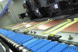
The process begins with the application of solder paste onto the PCB surface. Solder paste is a sticky mixture of tiny solder particles, flux, and other additives. It is precisely printed onto the PCB pads using a stencil or screen printer, creating a well-defined pattern for component placement. - Component Placement
Once the solder paste is printed, specialized pick-and-place machines are used to accurately place the SMD components onto the PCB. These machines use vision systems and highly precise motion control to position each component correctly on the solder paste deposits. - Reflow Soldering
After component placement, the PCB assembly enters a reflow oven or soldering machine. This oven subjects the assembly to a carefully controlled temperature profile, causing the solder paste to melt and create solid metallic interconnections between the component terminations and the PCB pads. - Inspection and Testing
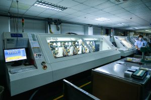
Following the reflow soldering process, the assembled PCBs undergo various inspection and testing procedures to ensure quality and functionality. Automated optical inspection (AOI) systems use cameras and image processing algorithms to detect defects such as misaligned components, solder bridges, or insufficient solder joints. Additional tests, like in-circuit testing (ICT) or functional testing, may also be performed to verify the electrical integrity and overall performance of the assembled PCBs.
Throughout the SMT assembly process, strict cleanliness and environmental controls are essential to maintain high product quality and yield. Factors such as temperature, humidity, and electrostatic discharge (ESD) must be carefully monitored and controlled to prevent defects and ensure consistent and reliable assemblies.
The SMT assembly process is highly automated, enabling high production volumes and consistent quality. However, it also requires skilled operators, specialized equipment, and robust quality control measures to achieve successful and reliable surface mount assemblies.
SMT Components
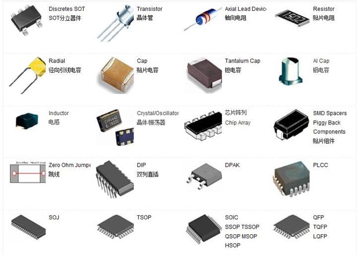
SMT assembly relies on a wide variety of electronic components designed specifically for surface mount applications. These components, known as SMDs, are characterized by their compact sizes, high lead counts, and specialized termination styles suited for soldering directly onto the PCB surface.
- Chip Components
Chip components, such as resistors, capacitors, and inductors, are among the most common SMT components. They are tiny, rectangular or cylindrical components without leads, designed to be mounted directly onto the PCB surface. - Flat Packages
Flat packages, like Quad Flat Packages (QFPs), Quad Flat No-leads (QFNs), and Land Grid Arrays (LGAs), are surface mount integrated circuits with leads or terminations arranged around the perimeter or underneath the package body. - Ball Grid Arrays (BGAs)
Ball Grid Arrays (BGAs) are advanced SMT packages with a grid array of solder balls underneath the component body, allowing for high-density interconnections and space-saving designs. - Small Outline Packages
Small Outline Packages (SOICs, SSOPs) are gull-wing or J-lead components designed for surface mount applications, offering a balance between size and lead count.
These SMT components come in various package sizes, lead counts, and termination styles to accommodate different circuit densities, power requirements, and design constraints. The terminations or leads of SMT components are designed for solder joint formation directly on the PCB surface, enabling compact and high-density assemblies.
Choosing the right SMT components is crucial for successful surface mount assemblies, as their physical characteristics, electrical properties, and thermal requirements must be carefully considered during the design phase. Additionally, proper component footprint and pad designs on the PCB are essential for reliable solder joint formation and long-term mechanical integrity.
SMT Equipment and Machinery
Successful SMT assembly requires specialized equipment and machinery to handle the intricate processes involved. From solder paste printing to component placement and reflow soldering, each step demands precise and automated systems to ensure consistent quality and high production throughput.
- Automated Pick-and-Place Machines
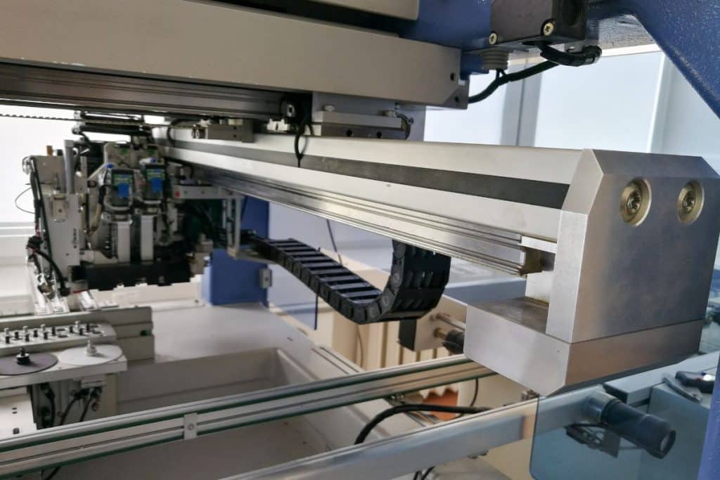
At the heart of the SMT assembly process are automated pick-and-place machines. These highly sophisticated systems use vision systems, precision motion control, and advanced robotics to accurately pick up individual SMT components from feeder reels or trays and place them onto the PCB with exceptional speed and accuracy. - Reflow Ovens
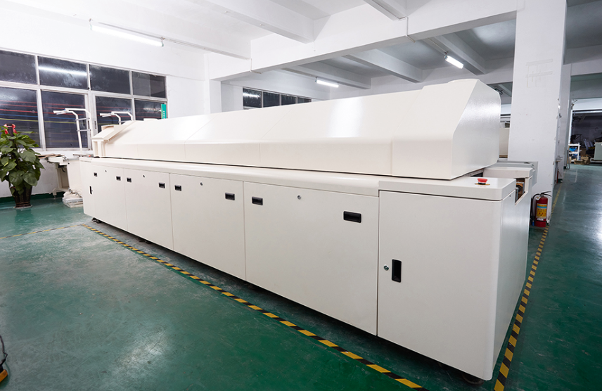
Reflow ovens, also known as reflow soldering machines, are essential for creating reliable solder joints between the SMT components and the PCB. These ovens subject the assembled PCBs to a carefully controlled temperature profile, causing the solder paste to melt and form solid interconnections. Advanced reflow ovens feature multiple heating zones, precise temperature control, and controlled atmospheric conditions to ensure optimal soldering results. - Solder Paste Printers
Solder paste printers play a crucial role in the SMT assembly process by precisely depositing solder paste onto the PCB pads. These printers use stencils or screens to create a well-defined pattern of solder paste for component placement. Accurate paste deposition is critical for ensuring proper solder joint formation and avoiding defects like solder bridges or insufficient solder. - Inspection Equipment
Quality control is paramount in SMT assembly, and various inspection equipment is employed to detect and prevent defects. AOI systems use high-resolution cameras and advanced image processing algorithms to inspect the PCB assemblies for issues such as misaligned components, solder defects, or missing components. Additionally, X-ray inspection systems and Automated X-ray Inspection (AXI) can be used to analyze the internal structure and quality of solder joints, particularly for dense assemblies or BGA components.
These specialized SMT equipment and machinery are designed to handle the intricate demands of surface mount assembly, ensuring high accuracy, repeatability, and throughput. However, proper setup, calibration, and maintenance of these systems are crucial to achieving optimal results and minimizing defects in the assembled PCBs.
Applications of SMT Assembly
SMT assembly has revolutionized the electronics industry, enabling the development of compact, high-performance, and reliable products across a wide range of applications. Here are some of the key industries and products that benefit from SMT assembly:
- Consumer Electronics
The consumer electronics industry is one of the primary drivers of SMT adoption. Devices such as smartphones, tablets, laptops, televisions, and wearable technology rely heavily on SMT assembly to achieve miniaturization, high component density, and advanced functionality. - Telecommunications
The telecommunications sector utilizes SMT assembly extensively to produce networking equipment, routers, modems, and other communication devices. SMT’s ability to accommodate high-frequency components and dense interconnects is crucial for meeting the ever-increasing demands for faster data transfer rates and higher bandwidths. - Automotive Electronics
Modern vehicles are equipped with numerous electronic control units (ECUs) and advanced driver assistance systems (ADAS), all of which rely on SMT assembly for compact and reliable electronic modules. SMT components are used in everything from engine control units to infotainment systems, ensuring efficient and safe vehicle operation. - Aerospace and Defense
The aerospace and defense industries demand highly reliable and compact electronic systems. SMT assembly is widely used in the production of avionics, navigation systems, radar systems, and other critical aerospace electronics, where miniaturization, weight reduction, and durability are paramount. - Medical Devices
The medical device industry benefits from SMT assembly in the manufacturing of various diagnostic and therapeutic equipment. From patient monitoring devices to implantable medical devices, SMT ensures compact and reliable electronic components that meet stringent safety and performance requirements. - Industrial Automation
SMT assembly plays a vital role in the development of industrial automation systems, including programmable logic controllers (PLCs), human-machine interfaces (HMIs), and robotics controllers. The compact and reliable nature of SMT assemblies contributes to these critical industrial components’ efficient operation and durability.
As technology continues to advance, the applications of SMT assembly are expected to grow even further, enabling the creation of smaller, more powerful, and more efficient electronic devices across numerous industries.
Challenges and Best Practices in SMT Assembly
While SMT assembly offers numerous advantages, it also presents several challenges that must be addressed to ensure reliable and high-quality assemblies. Overcoming these challenges requires adherence to best practices and implementation of robust quality control measures.
Challenges in SMT Assembly:
- Component handling and placement accuracy: Handling and precisely placing miniaturized SMT components can be challenging, especially for components with high lead counts or fine pitch packages.
- Solder defects: Improper solder paste deposition, inadequate reflow profiles, or contamination can lead to defects such as solder bridges, insufficient solder joints, or tombstoning (components standing up instead of lying flat).
- Thermal management: Proper thermal management is crucial during the reflow soldering process to ensure even heating and cooling, preventing issues like component cracking or delamination.
- Electrostatic discharge (ESD) control: SMT components are susceptible to ESD damage, making ESD control measures essential throughout the assembly process.
- Inspection and testing: Inspecting and testing dense SMT assemblies for defects can be challenging, requiring advanced inspection equipment and methodologies.
Best Practices for Successful SMT Assembly:
- Component selection and footprint design: Carefully selecting appropriate SMT components and designing optimal footprints on the PCB can significantly improve assembly quality and reliability.
- Solder paste printing optimization: Proper stencil design, solder paste selection, and printer setup can ensure accurate and consistent solder paste deposition.
- Reflow profile optimization: Developing and adhering to optimized reflow profiles tailored to the specific assembly requirements is crucial for achieving high-quality solder joints.
- Strict environmental controls: Maintaining controlled environments for temperature, humidity, and ESD protection is essential for successful SMT assembly.
- Comprehensive inspection and testing: Implementing rigorous inspection and testing protocols, including AOI, X-ray inspection, and functional testing, can identify and prevent defects.
- Process control and continuous improvement: Continuously monitoring and improving the SMT assembly process through statistical process control (SPC) and data analysis can enhance quality and yield.
By addressing these challenges and following industry best practices, manufacturers can achieve consistent, reliable, and high-quality SMT assemblies, enabling the production of cutting-edge electronic products that meet the demanding requirements of various industries.
Environmental Impact of SMT Assembly
As the electronics industry continues to grow, it is crucial to consider the environmental impact of manufacturing processes, including SMT assembly. Fortunately, the SMT industry has made significant strides in adopting environmentally responsible practices and addressing potential concerns.
- Lead-Free Soldering
One of the most significant environmental initiatives in SMT assembly is the transition to lead-free soldering. Traditional solder alloys containing lead pose significant health and environmental risks due to their toxicity. To mitigate these risks, the electronics industry has widely adopted lead-free solder alloys, such as tin-silver-copper (SAC) and tin-copper (SnCu), which are more environmentally friendly and comply with various global regulations. - Material and Component Recycling
SMT components and PCB assemblies contain valuable materials, including metals, plastics, and ceramics. Proper recycling and material recovery processes can significantly reduce the environmental impact of SMT assembly by minimizing waste and conserving natural resources. Many electronics manufacturers and recycling facilities now have dedicated programs for responsibly recycling and recovering materials from obsolete or defective SMT assemblies. - Energy Efficiency
SMT assembly processes, particularly reflow soldering, can be energy-intensive. However, advancements in equipment design and process optimization have led to more energy-efficient SMT assembly lines. Modern reflow ovens and other machinery are designed to minimize energy consumption while maintaining precise process control, reducing the overall environmental footprint of SMT manufacturing. - Reduced Material Consumption
The inherent miniaturization of SMT components and high-density assemblies results in reduced material consumption compared to traditional through-hole technology. Smaller components and compact designs require less raw material, contributing to resource conservation and waste reduction.
While the SMT industry continues to make progress in addressing environmental concerns, ongoing efforts are required to further improve sustainability practices. This includes exploring more eco-friendly materials, implementing closed-loop recycling systems, and adopting renewable energy sources to power SMT assembly lines.
By embracing environmentally responsible practices, the SMT industry can contribute to a more sustainable future while meeting the ever-growing demand for advanced electronic products.
Future Trends in SMT Technology
The field of SMT is continuously evolving, driven by the relentless demand for smaller, more powerful, and more efficient electronic devices. As we look to the future, several exciting trends are shaping the SMT industry:
- Miniaturization and Smaller Packages
The pursuit of miniaturization remains a driving force in SMT technology. Component manufacturers are constantly pushing the limits of package sizes, introducing even smaller and more compact designs. Chip-scale packages (CSPs), wafer-level packaging (WLP), and the emerging panel-level packaging technologies are enabling unprecedented levels of miniaturization, allowing for higher component densities and more advanced product designs. - 3D Packaging and Through Silicon Via (TSV)
To address the challenges of miniaturization and performance, the industry is exploring innovative 3D packaging solutions. Through Silicon Via (TSV) technology enables the vertical stacking of multiple dies or chips, creating high-density 3D integrated circuits (3D ICs). This approach not only reduces the overall package footprint but also shortens interconnect lengths, improving signal integrity and performance. - New High-Density Interconnect Technologies
As component densities continue to increase, traditional surface mount interconnects may reach their limits. To address this challenge, new high-density interconnect technologies are being developed, such as embedded trace substrates and fan-out wafer-level packaging (FO-WLP). These advanced techniques enable finer-pitch interconnects and higher I/O densities, facilitating the integration of more functionality within a smaller footprint. - Advanced Materials and Substrates
Researchers are exploring new materials and substrate technologies to enhance SMT assembly performance and reliability. For example, the use of low-loss substrates and advanced dielectric materials can improve signal integrity and reduce electromagnetic interference (EMI) in high-frequency applications. Additionally, the development of flexible and stretchable substrates opens up new possibilities for wearable and conformal electronics. - Industrial 4.0 and Smart Manufacturing
The SMT industry is embracing the principles of Industry 4.0 and smart manufacturing, leveraging technologies such as the Internet of Things (IoT), big data analytics, and artificial intelligence (AI). Smart SMT assembly lines with interconnected machinery, real-time monitoring, and predictive maintenance capabilities can optimize processes, improve quality, and increase efficiency.
As these trends continue to shape the SMT industry, we can expect more innovative and cutting-edge electronic products that push the boundaries of what is possible in terms of size, performance, and functionality. Staying ahead of these trends will be crucial for manufacturers and suppliers involved in SMT assembly to remain competitive in the ever-evolving electronics landscape.
Conclusion
SMT assembly has transformed the electronics industry, enabling the creation of incredibly compact, high-performance, and reliable electronic devices that have become an integral part of our daily lives. From smartphones and laptops to medical equipment and aerospace components, SMT assemblies are at the heart of modern technological marvels.
Throughout this comprehensive guide, we have explored the intricacies of SMT assembly, delving into its processes, components, equipment, and applications. We have witnessed how this technology has revolutionized electronics manufacturing, allowing for miniaturization, cost-effectiveness, and enhanced reliability.
As we look to the future, the SMT industry continues to push the boundaries of innovation, with exciting trends such as 3D packaging, advanced materials, and smart manufacturing on the horizon. These developments will further enable the creation of smaller, more powerful, and more efficient electronic products, driving the next generation of technological advancements.
However, it is essential to recognize that the pursuit of technological progress must be balanced with environmental responsibility. The SMT industry has made significant strides in adopting environmentally friendly practices, such as lead-free soldering, material recycling, and energy efficiency initiatives. Continued efforts in this direction will ensure a sustainable future for the electronics manufacturing industry.
Partnering with a reliable and experienced PCB assembly service provider is crucial for businesses seeking to stay ahead in the competitive electronics market. At JHYPCB, we offer comprehensive SMT assembly services, leveraging state-of-the-art equipment, stringent quality control measures, and a team of highly skilled professionals. Our commitment to excellence ensures that your electronic products are assembled with the highest standards of quality, reliability, and efficiency.
If you have any questions or would like to discuss your SMT assembly requirements, please don’t hesitate to contact us. Our team of experts is ready to assist you in navigating the world of surface mount technology and bringing your electronic designs to life.
FAQs on SMT Assembly
SMT involves mounting components directly onto the surface of the PCB, while through-hole assembly requires inserting component leads into drilled holes in the PCB.
Key advantages include smaller component sizes, higher component density, improved reliability, automated assembly, and cost-effectiveness.
Common SMT components include chip components (resistors, capacitors), flat packages (QFP, QFN), ball grid arrays (BGAs), and small outline packages (SOIC, SSOP).
Essential SMT equipment includes automated pick-and-place machines, reflow ovens, solder paste printers, and inspection systems like AOI and AXI.
Solder paste is precisely printed onto the PCB pads using a stencil or screen printer, creating a pattern for component placement.
Challenges include handling miniaturized components, solder defects, thermal management, ESD control, and inspection of dense assemblies.
The industry has adopted lead-free soldering, material recycling, energy efficiency measures, and reduced material consumption to mitigate environmental impact.
Trends include further miniaturization, 3D packaging, new interconnect technologies, advanced materials, and smart manufacturing (Industry 4.0).
Related Posts
- PCB Assembly Cost: A Comprehensive Guide for Cost-Effective PCB Manufacturing
- What is a PCB Manufacturer? The Definitive Guide
- Custom PCB Assembly Services for Low-Volume & Specialty Needs
- What is Lead-Free Solder Paste (Pb-Free) in PCB Assembly?
- 3 Special Reminders for Printed Circuit Board Assembly (PCBA)
- Shenzhen – The Global Hub for High-Quality PCB Assembly Manufacturing
- Evaluating and Selecting Quick-Turn PCB Assembly Manufacturers in China
- Leveraging Turnkey PCB Assembly Manufacturing Services
- Choosing the Right PCB Assembly Manufacturer for Your Needs
- What Is Prototype PCB Assembly?
- How to Get a Quote and Order PCB Assembly?
- Internal Flow of PCB Prototype Assembly
- Electronic PCB Assembly Process and Flow Chart
- How to Select the Right Low-volume PCB Assembly Manufacturer
- The Advantages and Disadvantages of Surface Mount Technology (SMT)
- Materials Used in Surface Mount Technology
- SMT PCB Assembly Manufacturing Process Introduces
- The Two Typical SMT Reflow Soldering Temperature Curve Modes
- What is the defference between PCB and PCBA?
- 30 Common SMT PCB Assembly Defects
- What is the difference between SMT and SMD?
- The Production Process and Specifications of PCB SMT stencil
- What is the Bill of Materials(BOM) and how to create one?
- The Main PCB Assembly Process Steps


