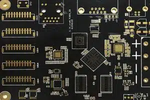
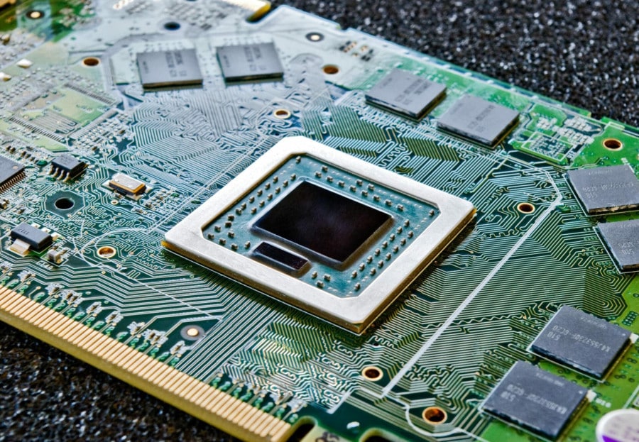
As printed circuit boards are designed to pack ever more components into increasingly compact spaces, manufacturers have developed innovative technologies to enable further miniaturization. One such technology is the microvia – a small via used to interconnect layers in high density PCBs.
Measuring typically between 0.005-0.015 inches (0.13-0.38mm) or less in diameter, microvias play a crucial role in reducing PCB thickness and layer count while maintaining performance. This allows more functionality to be integrated into ever-shrinking electronics hardware. From complex smartphones to nimble wearables and space-constrained internet of things (IoT) devices, microvia PCBs confer reliability in highly demanding environments.
The continual demand for smaller, faster, cheaper electronics means HDI and multilayer boards have become widespread in consumer and industrial electronics over the past decade. As traditional through-hole vias occupy substantial space and limit routing channels, they present obstacles to achieving further miniaturization, especially in interlayer connections.
By contrast, laser-drilled or photo-imageable microvias minimize disruptions in circuit routing while optimizing vertical interconnect access between layers. While microvia PCB technology brings considerable complexity around precision drilling, plating, and process control, the benefits outweigh the challenges. As electronics applications push the boundaries of technological capability, microvias play an indispensable, if microscopic, role.
Table of Contents
Types of Microvias
There are two primary technologies used for producing microvias in PCBs – laser drilling and photoimaging. Both enable small vias to interconnect board layers, though they differ in their processes and characteristics.
Laser-Drilled Microvias
Laser drilling uses a YAG, CO2 or excimer laser to selectively ablate material when fabricating a PCB. The technique can yield microvias down to 0.005 inches (0.13mm) and achieve high density on panel sizes up to 32 x 48 inches. Laser-drilled microvias offer two principal benefits:
- High precision with small capture pads: Laser systems can focus energy to a tight spot size, enabling very fine microvias with capture pads/annular rings down to 0.003 inches. This maximizes routing space for traces.
- Ability to meet depth ratio requirements: Depth-to-diameter ratios up to 15:1 are possible. This allows drilling through thick multilayer boards.
Photoimageable Microvias
Photoimageable techniques use UV light exposure to pattern microvias, followed by selective copper plating processes. Typical minimum microvia sizes are around 0.006 inches. Advantages include:
- Lower costs on lower-density boards: Avoiding laser systems reduces equipment expenses.
- Scalable production: Panel sizes up to 48” x 96” can be accommodated, though line/space rules tend to be more relaxed.
So in summary, laser drilling yields the smallest and densest microvia structures when precision and depth are paramount. Photoimaging offersreduced costs where ultra-fine features are not essential. Both constitute mature productionmethods for incorporating blind and buried microvias across myriad PCB applications.
Microvia PCB Technology
Creating reliable interconnections with microvias entails stringent fabrication processes. Key considerations around layered stacking, drilling, plating, and process control must be addressed.
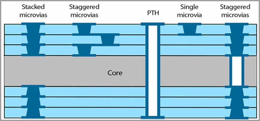
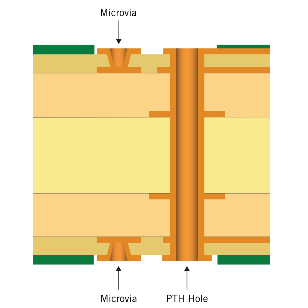
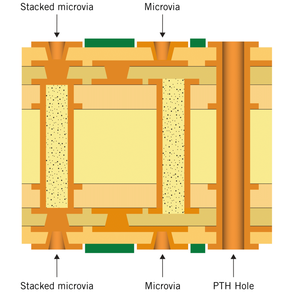
Stacked and Staggered Microvia Structures
Microvias can be configured vertically in stacked or staggered arrangements depending on connection needs:
- Stacked: Microvias line up directly between layers, occupying the same x-y space. This approach serves simpler vertical interconnections.
- Staggered: Offset microvias connect between layers in interlaced patterns. Staggering reduces mechanical stress while meeting more complex connectivity demands.
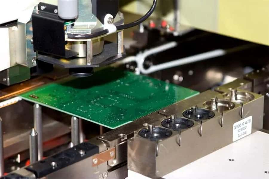
Precision Drilling
Laser drills must deliver tightly controlled energy pulses and precise positioning to bore thousands of microscopic vias across each board with minimal taper. Tight microvia placement also ensures adequate annular rings around each copper pad.
Metallization and Plating
Electroless copper processes deposit thin conformal seed layers of metal inside each microvia hole. A copper electroplating step then deposits thicker metal until the via is filled level with the pad surface. Complete, voids-free copper plating is critical for reliability.
Process Control
Maintaining integrity across drilling, metallization, and imaging steps is vital to maximizing production yield. Statistical process controls govern measuring microvia diameters, capture pad sizes, depth uniformity, and plating quality to stay within acceptable tolerances, driving towards 6 sigma capability levels.
By leveraging such disciplined methods, microvia PCBs balance cost controls while meeting rigid functionality benchmarks during volume manufacturing.
While disciplined microvia fabrication processes enable complex PCBs, the inherent stresses arising from thermal cycling, pad configurations, and environmental factors also impact overall reliability.
Microvia Reliability Factors
As with any PCB technology pushing miniaturization boundaries, microvias undergo substantial stresses, especially in demanding end-use environments. Key influences on reliability include:
Thermal Cycling Stresses
The coefficient of thermal expansion (CTE) mismatch between copper microvias, surrounding laminate materials, and pads produces mechanical strains during temperature changes that accumulate over time. Effects intensify as microvia dimensions keep decreasing.
Pad Size and Capture Pads
The pad area surrounding a microvia must sufficiently capture the interconnection during cycling stresses. Individual boards require optimization of capture pads size around each via. This is a function of layer count, total board thickness, and adjacent routing constraints.
Underfills and Encapsulants
Applying protective polymers helps counteract thermal expansion and moisture ingression threats. However, underfill viscosity must permit adequate flow rates to permeate high density microvia structures. Dispense methods also warrant consideration during assembly to avoid introducing voids which undermine protection.
By mitigating these factors during design reviews, production engineers help microvia PCBs meet functionality and longevity expectations within target application environments. Continual testing and failure analysis provides feedback for continual reliability improvements.
Once viewed as specialized technology, microvias now serve essential functions across virtually every electronics sector where miniaturization and reliability are baseline requirements.
Applications of Microvias
Consumer Electronics
From smartphones to tablets and wearables, microvias help embed antennas, build multi-layer system-on-chip (SoC) packages, and interconnect high density PCBs while averting buried vias.
Automotive Electronics
Miniaturized circuits manage greater automotive functionality in tighter spaces even as environmental demands escalate. Microvias support evolving electronic content per vehicle.
Aerospace and Defense
Rigorous quality standards and extended operating lifetimes rule aerospace applications. Microvias integrate guidance systems and sustain G-forces in severe conditions.
Medical Devices
Connecting multilayer rigid-flex-rigid PCBs which contour human anatomy motivates microvias in ultrasound transducers, implanted devices and other instruments.
Emerging Applications
The inherent scalability of consumer IoT networks and their edge devices will depend on microvia PCBs as complex circuitry migrates towards self-learning capability.
Every new product generation seems to intensify requirements for electronics functionality. As such, microvias continue seeing exponential global adoption across industries where metrics for speed, efficiency, and intelligence are ever-rising.
Already firmly entrenched across key technology sectors, innovations in microvia fabrication and integration will drive next-generation applications where small size and high density help unlock greater electronics potential.
The Future of Microvias
Projected Advancements
Continued developments in laser direct imaging and drill technology will facilitate smaller microvias with higher aspect ratios. This will reduce layer counts in complex boards. Tighter process controls aim to double production yields within 5 years.
Contribution to Miniaturization
As consumer devices converge functionalities, microprocessors combine more components and sensors onto single chips. Microvias will interconnect these high density configurations where functionality trumps footprint.
Role in HDI & Multilayer PCBs
High density interconnect PCBs with 6-12+ layers will demand proven microvia reliability to realize space savings, just as smartphones pioneered over the last decade. And as exotic substrates like flex-rigid blends gain adoption across industries, microvias will serve critical anchoring functions.
By scaling down dimensions while ramping up precision execution, the continual advancement of microvia integration will unleash space, speed and efficiency gains to tackle some of electronics’ greatest multi-disciplinary challenges in the years ahead.
As microvia PCB technology migrates from early stage innovation into widespread global implementation, having an experienced manufacturing partner is instrumental in reaping benefits while mitigating complexities.
JHYPCB's Capabilities in Microvias
Equipment and Expertise
JHYPCB operates advanced laser drilling and imaging equipment to fabricate microvias on panel sizes over 30 inches. Our engineering team brings decades of know-how in optimizing microvia builds for reliability and performance.
Volume Production Experience
We have manufactured over 500,000 microvia boards annually, becoming proficient in scalability while adhering to strict quality protocols across local and exported volumes.
Quality Control
100% AOI inspection combined with intensive process auditing enables JHYPCB to meet demanding application requirements from automotive suppliers and defense contractors alike. We benchmark against the industry’s highest microvia DFM and DFR standards.
Fast Prototypes to Cost-Effective Production
By synthesizing technical expertise with responsive customer service and expedited logistics, JHYPCB delivers microvia innovation with rapid prototypes while competing vigorously on high volume production runs.
As next-generation microvia performance barriers are defined by novel devices and mission-critical systems alike, manufacturers will continually innovate while enhancing yields. With seasoned high-reliability expertise and efficient large-scale output, JHYPCB stands ready to partner and deliver.
Related Reading