sales@pcbjhy.com

Sales Manager: Ms. Megan

+86-13825274100

24/7 Customer Support

+86-13825274100

WeChat and WhatsApp

Knowledge of Flexible PCB Manufacturing Process Steps

PCB is the necessary product of the electronic industry. Flexible PCB is a broad category of PCBs. According to the structure of FPC, it can be divided into a single-layer, double-sided, and multilayer flexible PCB according to the number of conductor layers.
Flexible PCB Manufacturing Process flowchart

Flexible Printed circuit (FPC) Overview

What is Flexible PCB?

Printed circuit boards(PCBs) are the necessary products of the electronic industry.

They are widely used in electronic products such as communication equipment, computers, automotive electronics, industrial equipment, and various household appliances. Their main functions are to support circuit components and interconnect circuit components. FPC(Flexible Printed Circuit Board) is a broad category of PCBs. According to the structure of FPC, it can be divided into a single-layer, double-sided, and multilayer flexible PCB according to the number of conductor layers.

FPC-Flexible Printed Circuit Board
Flexible PCB Assembly

The Types and stack up of Flexible PCB

There are several types of flexible circuit boards as follows: 

The structure of FPC Flexible PCB

① The Single-sided flexible circuit board is the lowest-cost printed circuit board that does not require high electrical performance. For a single-sided layout, a single-sided FPC should be used. It has a layer of chemically etched conductive patterns, and the conductive pattern layer on the surface of the flexible insulating substrate is a rolled copper foil. The insulating substrate can be polyimide, polyethylene terephthalate, aramid cellulose ester, and polyvinyl chloride.

Single-sided Flexible PCB Stack up
Double-sided Flexible PCB Stack up

② The double-sided flexible circuit board is a conductive pattern made by etching on both sides of the insulating base film. The metalized hole connects the models on both sides of the insulating material to form a conductive path to meet the design and use the function of flexibility. The cover film can protect single and double-sided wires and indicate where the components are placed.

③ The Multi-layer flexible circuit board is to laminate 3 or more layers of single-sided or double-sided FPC flexible circuit boards together and form metalized holes by drilling and electroplating to form conductive paths between different layers. In this way, no complicated welding process is required. Multilayer circuits have vast functional differences in higher reliability, better thermal conductivity, and more convenient assembly performance. When designing the layout, the mutual influence of assembly size, the number of layers, and flexibility should be considered.

Multilayer Flexible PCB Stack up
Rigid-flex PCB Stack up

④The traditional rigid-flex PCB board is composed of rigid and flexible substrates selectively laminated together. The structure is compact, and the metalized hole forms a conductive connection. If there are components on the front and back of a printed board, a rigid-flex PCB is the right choice. But if all the parts are on one side, it will be more economical to choose a double-sided flexible PCB and laminate a layer of FR4 reinforced material on its back.

⑤Air Gap flexible PCB. (Single-sided CCL (circuit) + pure glue + single-sided CCL) + Top and Bottom cover layer (CVL)
Note: After bonding the two single-sided copper foils with pure glue, use the PTH hole to make the two layers conductive.

Air Gap Flexible PCB Stack up
Sculptural Flexible PCB

⑥Sculptural Flexible PCB. Pure copper foil+Top and bottom cover layer (CVL)
Description: Press thicker pure copper foil on the PI to form a floating, finger structure in a local area; it is mostly used for crimping liquid crystal display (TFT) and can provide plug-in functions for dense welding.

Which material is used in flexible PCB?-Main Raw Materials for FPC

1) Flexible copper clad laminate (FCCL): According to the difference between one side covered with copper foil or both sides covered with copper foil, it is called single-sided copper-clad laminate and double-sided copper-clad laminate; according to the difference between the copper foil and the base film whether there is an adhesive, It is called glued copper-clad laminate and glueless copper clad laminate. The substrate films of flexible copper clad laminates are commonly used polymer films such as PI, PET, PEN, and LCP. The copper-clad laminate is mainly responsible for conduction, insulation, and support on the entire printed circuit board. The performance, quality, processability in the manufacturing process, manufacturing cost, and manufacturing level of printed circuit boards depend to no small extent on the production of copper-clad laminates.

(2) Cover Lay: It is composed of organic film and adhesive. The function of the cover film is to protect the completed flexible circuit conductor part. Adhesive films have different substrate film and adhesive types and thickness specifications. Some flexible printed circuit boards do not use cover film on the surface but use solders to reduce costs.

Cover Lay Structure

(3) Adhesive: It is formed by pouring adhesive on both sides or one side of a substrate film. There are also adhesive films with a transparent adhesive layer without substrate. The sticky film has different adhesive types and thickness specifications. The sticky film is used for interlayer adhesion and insulation of multilayer boards.

Structure of adhesive

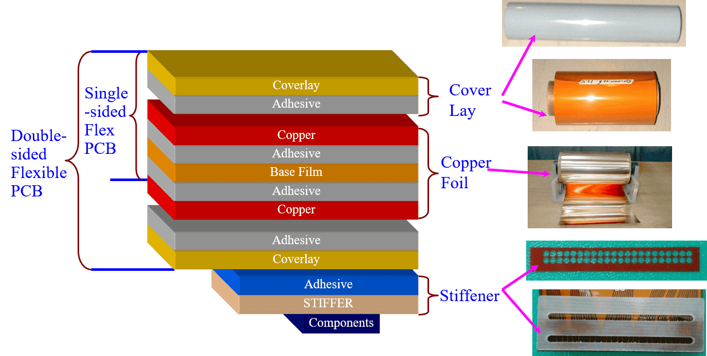
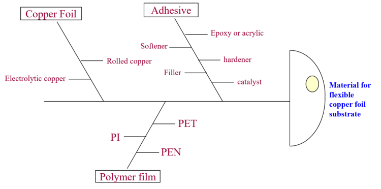
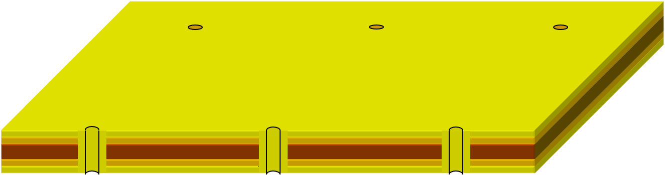
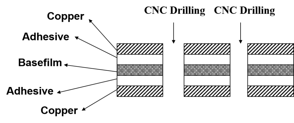
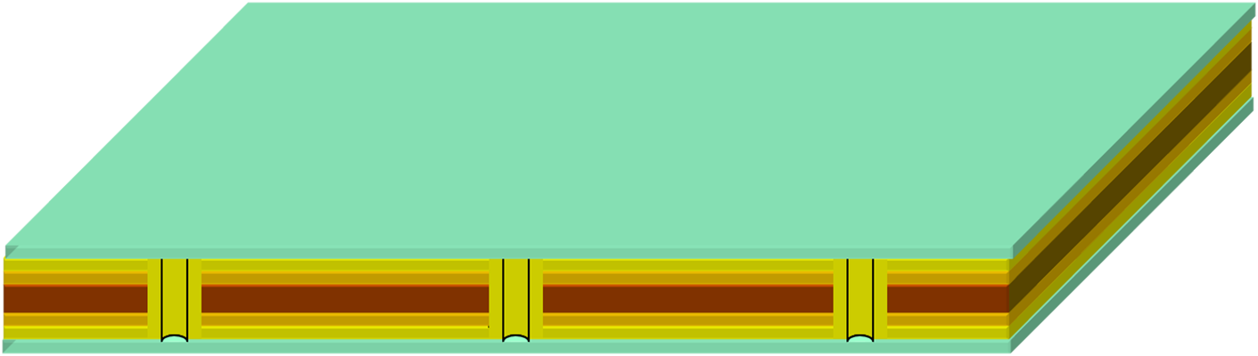
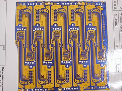
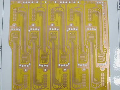
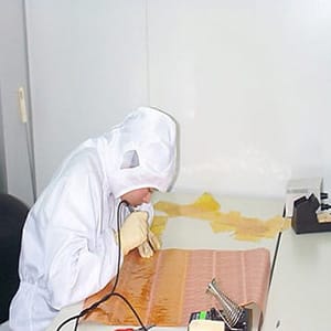
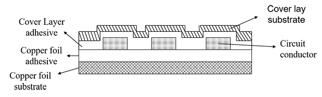
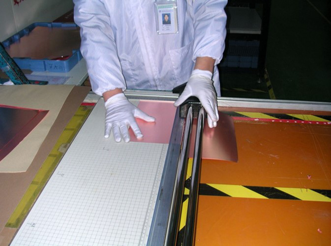
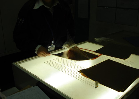
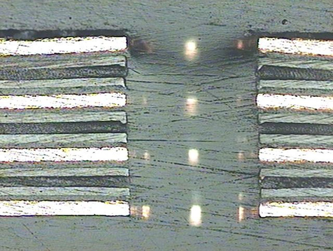
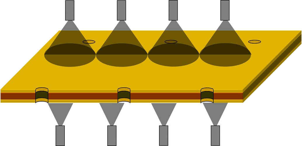
(4) Copper foil: There are electrolytic copper foil and rolled copper foil and different copper foil thickness specifications. Copper foil is used for the two surface conductor layers in the production of multilayer printed circuit boards.

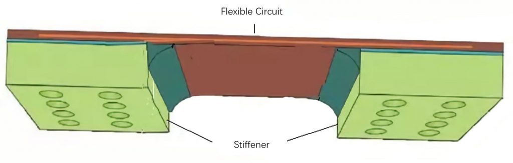
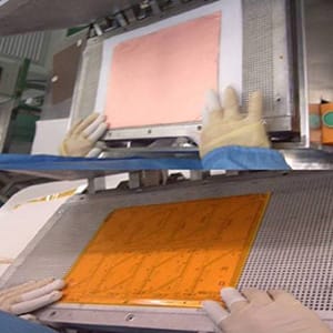
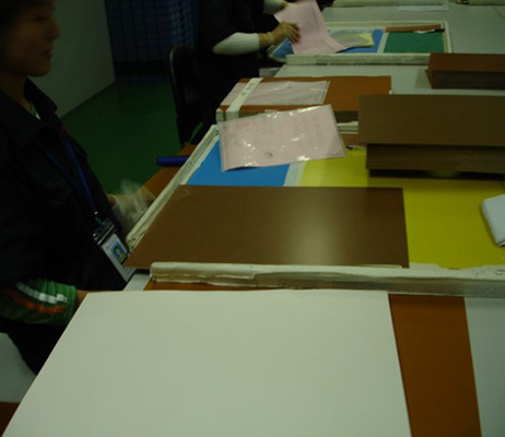
Besides, some FPC flexible printed circuit boards use stiffener materials, such as metal sheets, plastic sheets, resin films, and epoxy glass substrates. The role of the reinforcing material is to reinforce a part of the flexible circuit board for support and fixation.

FPC flexible printed circuit board with stiffeners

Flexible PCB Manufacturing Process Steps

Flexible printed circuit board processing uses the same process and similar equipment conditions as rigid PCB boards. In the form of processing, there is sheet-by-sheet processing, which is identical to the intermittent and step-by-step processing of rigid boards, or Roll to Roll, which is the continuous processing of a roll of the substrate.

Single-sided Flexible PCB Manufacturing Process

Cutting → Drilling → Dry Film Lamination → Position and Exposure → Develop → Etching → Remove Dry Film → Surface Finish → Coverlay Lamination →Lamination → Curing → Surface Finish → Immersion Gold → Silkscreen → V-cutting/scoring → Electrical Test → Punching → FQC → Packaging → Shipment

Double-sided Flexible PCB Manufacturing Process

Cutting → Drilling → PTH → Electroless Plating → Pretreating → Dry Film Lamination → Position → Exposure → Develop → Pattern Plating → Remove Dry Film → Pretreating → Dry Film Lamination → Position and Exposure → Develop → Etching → Remove Dry Film → Surface Finish → Coverlay Lamination → Lamination → Curing → Immersion Gold → Silkscreen → V-cutting/scoring → Electrical Test → Punching → FQC → Packaging → Shipment

Download the single-layer flexible PCB manufacturing process and double-sided Flex PCB manufacturing process ppt and PDF.

STEP 1: Cutting of Flexible Copper Clad Lamination

  • Generally, flexible circuit board materials are primarily manufactured in rolls. To meet the requirements of different sizes of products, it is necessary to plan and design the best utilization rate according to different product sizes. According to the planning results, the materials are cut into the required size.
  • Use a cutting machine to cut the rolled copper foil into a semi-finished copper foil sheet of the required size.

STEP 2: CNC Drilling

According to customer needs, the through-holes are drilled by mechanical drilling. According to different needs, various holes are equipped with different diameters. The pore diameter of PTH holes varies with customer requirements.

The types of holes are positioning holes, test holes, part holes, and PTH.

Recommended Reading: Plated Through Hole, Blind Via, and Buried Via in PCB Fabrication

STEP 3: Plasma etchback

The purpose of plasma etchback is to remove the residual glue on the hole wall and the residual foreign matter on the surface of the multi-layer board after drilling.

STEP 4: Shadow / Black Hole

  • Purpose: Deposit a layer of carbon powder on the glue of the hole wall of the electrochemical hole, which will play a conductive role during electroplating.
  • The black hole line uses the principle of carbon powder to be conductive,and positive and negative to attract, and the carbon layer is evenly attached to all the hole walls.

STEP 5: Chemical cleaning

Purpose:

  • Chemical cleaning can remove oxides, oil stains, and impurities on the surface of the copper foil.
  • Roughen the circuit board surface

Chemical cleaning
Chemical cleaning

STEP 6: Plating Through Hole

The upper and lower conductors are not connected after the double/multilayer board material is drilled mechanically. A conductive layer must be plated on the wall of the drilled hole to make the signal conductive. There is no such process in single-sided flexible circuit boards.

The ring-shaped electroplating line adopts the principle that the phosphor copper ball anode precipitates copper ions after power-on, and the cathode absorbs copper ions, and the copper ions are uniformly deposited on the surface of the hole wall to achieve the purpose of electrical conduction between the hole wall and the surface of the product.

Plating Through Hole
PTH

STEP 7: Dry Film Lamination

Dry film: A photosensitive resist for etching or electroplating. It is composed of polyester film, photoresist film, and polyethylene protective film.

Purpose: Use a hot roller to evenly cover the dry film on the copper foil substrate to provide image transfer.

Using a heated roller with appropriate pressure, the hot-melt dry film is melted in a short time and then evenly filled on the surface of the product, which provides conditions for image transfer on the negative during subsequent exposure operations.

STEP 8: Exposure

Exposure is to use the characteristics of the dry film to make the product specifications into a negative film, through the principle of photographic exposure, to achieve the effect of image transfer.

The principle of exposure is that the initiator absorbs the light energy and decomposes it into free radicals under the irradiation of ultraviolet light. The free radicals initiate the polymerization and cross-linking reaction of the photopolymerizable monomers. After the reaction, a macromolecular structure insoluble in dilute alkali solution is formed.

The working film for exposure is a negative film, and the hollow and transparent part is the circuit and the copper area.

Operating environment: yellow light area.

STEP 9: Development

The developer is used to changing the exposed dry film to form a circuit chemically.

STEP 10: Pattern Etching

The developed material will be rinsed with an etching solution to remove the exposed copper layer that has not been protected by the dry film, leaving behind the protected circuit.

Operating principle: etching chemical reaction formula (regeneration reduction reaction)

STEP 11: Dry Film Stripping

After etching the material, there is still a hardened dry film on the board. The film stripping process is used to completely separate the dry film from the material so that the circuit is completely exposed and the copper layer is completely exposed.

 STEP 12: AOI
Automatic optical inspection instrument to check the circuit for short circuit or open circuit… etc.

Recommended Reading: Testing & Inspection Methods For PCB And PCBA

STEP 13: Cover Layer (CVL) / Pre Lamination

Paste a protective film on the surface of the circuit board to prevent the circuit from being oxidized and scratched and play a protective role.

STEP 14: Hot Press Lamination

Press the CCL, CVL, reinforcement sheet, etc., to fit together under high temperature and high pressure tightly.

STEP 15: Surface Finish

Plating the exposed copper foil with tin or gold can avoid oxidation and make it easier to solder parts.

According to customer requirements, electroplating or chemical deposition is used for the surface finish in the PAD area. At present, the common surface finish methods are gold plating, immersion gold, tinned copper, immersion tin and OSP (organic solder protection film), and other surface finish methods.

STEP 16: Silkscreen

Print text ink, silver paste, or solder resist ink on semi-finished products. Silver paste is usually used for shielding. After the silver paste is printed, it must be printed with a solder mask for protection.

STEP 17: O/S Testing

Use the probe to test whether there are any undesirable phenomena such as open circuit/short circuit.

Learn more about what is flying probe test?

STEP 18: Punching/Routing

The entire panel is cut into a single piece using steel mold/die or laser cutting and finally cut into a shape consistent with the customer’s design.

STEP 19: Inspection

Measure the appearance size and inspect the appearance (the methods used include visual inspection, microscope, magnifying glass, etc.)

Inspection
Visual inspection

STEP 20: Packaging

When the flexible circuit board is shipped, the packaging method will be determined according to different customer needs and external dimensions to ensure that the product is not damaged during transportation.

Tips for packaging:
1. Vacuum packaging
2. Low adhesion packaging material
3. Standard vacuum box/Tray
4. Dedicated vacuum box/Tray (antistatic grade)
5. Put cardboard between each piece of FPC
6. Put in the humidity indicator card
7. Paste the production date, packaging quantity, and other signs

How are flexible PCBs manufactured?

Flexible printed circuit manufacturing procedure

Flexible PCB Manufacturing & Flex Circuit Assembly

About Me

JHYPCB is a leading PCB prototyping, PCB manufacturing and assembly service provider in China, offering quick turn PCB prototyping, multi-layer PCB manufacturing and turnkey PCB assembly services.

Recent Posts

PCB assembly service
Scroll to Top