
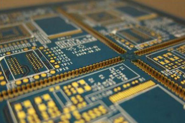
PCB Solder Mask
The most comprehensive Introduction of Solder Resist for PCB
Home » PCB Manufacturing » PCB Solder Mask
Table of Contents
1. What is Solder Mask in PCB?
In the world of printed circuit board design and manufacturing, the solder mask plays a crucial role in ensuring the reliability and longevity of electronic devices. This protective coating, often referred to as solder resist or solder stop, is applied to the surface of PCBs to prevent solder bridges and oxidation during assembly.
The solder mask serves several key functions. Firstly, it protects the copper traces and other exposed metallic components from environmental factors such as moisture, chemical exposure, and abrasion. By creating an insulating barrier, the solder mask safeguards the integrity of the circuit and prevents short circuits or other potential failures.
Secondly, the solder mask provides a visual aid during the inspection and assembly stages. Its distinctive color (often green) creates a high-contrast background, making it easier to identify components, pads, and other features on the PCB surface. This aids in manual inspection and AOI processes, reducing the risk of manufacturing defects.
Furthermore, the solder mask plays a crucial role in controlling the flow of molten solder during the assembly process. By creating openings (often referred to as solder mask defined pads) around the component pads and other areas where solder is intended to flow, it helps prevent solder bridging and ensures proper solder joint formation.
With the increasing miniaturization of electronic components and the demand for high-density interconnects, selecting the appropriate solder mask type and thickness has become more critical than ever. Various solder mask options are available, each with its own advantages, limitations, and compatibility with different manufacturing processes and end-use applications.
Exactly speaking, a solder mask can also be called the “Protection Layer” of PCBs. Besides, the solder mask also has the following functional characteristics:
- Cost-effective coating
- For Aesthetics purpose
- Excellent mechanical and chemical properties
- Various colors for choice to meet all kinds of customer’s needs
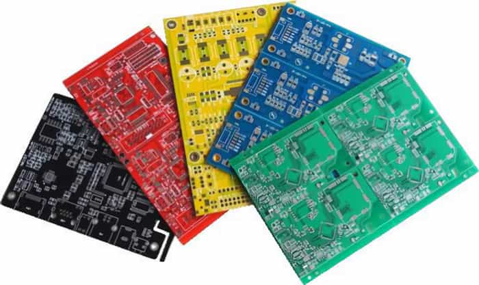
What color of solder mask is used on the PCB?
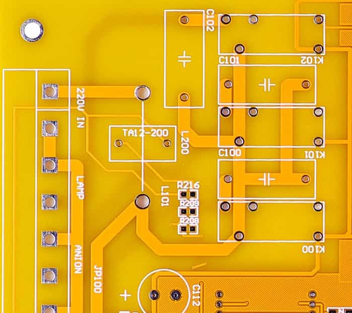
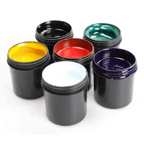
PCB Solder Mask Colors
As you know, green is the most common color for solder mask, but there are many other colors available. Some colors JHYPCB also uses:
- Green
- Red
- Blue
- Yellow
- White
- Black
- Matte Green
- Matte Black
- Purple
- Green Solder Mask
For many years the only solder mask color you could see on a printed circuit board was green. Why is Green Solder mask only solder mask color early? Why didn’t we start with blue, yellow, or red solder masks? There are several possible reasons for reference.
Why are PCBs green?
1) It goes back to the old military requirements, that the solder mask must be green.
2) Solder mask is green because when it was originally produced, the base resin was brownish-yellow in color, and the hardener was very muddy brown, and when you mixed them, you got green. Also, laminates at that time were mostly green. So it was easy to accept the idea of a green solder mask as well.
3) That particular shade of green produced the right contrast with the white legend ink while being tested under all types of adverse conditions.
4) Green has been proven to be the color most visible to the human eye.
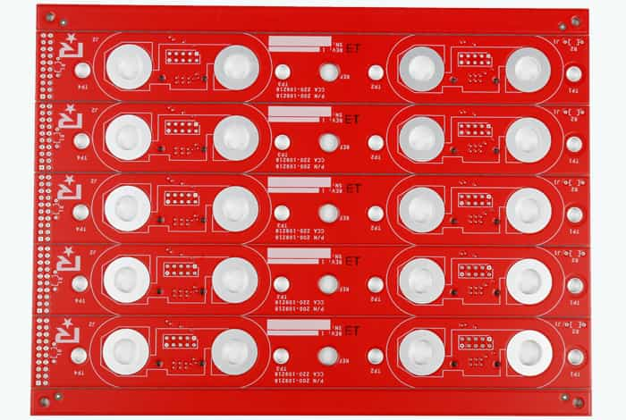
- Red Solder Mask
Red Solder Resist is bold, and it looks professional. The contrast between traces, planes, and space is good but observably lower than on a green board. Inspection of fine traces on the board for defects is best done with some form of magnification. Silkscreen stands out well against the red background, and flux residues clean up well, just as well as on a green board.
Though there is no significant difference between a green solder mask and red solder mask, Red Solder Resist is eye-catching. If you want an outstanding board, you can try a red solder mask.
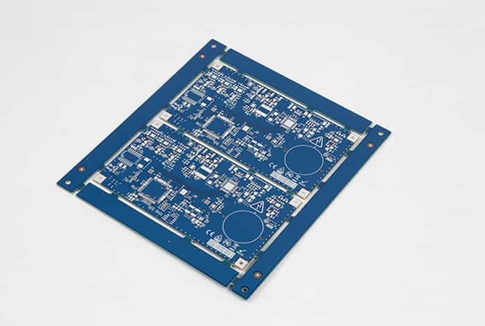
- Blue Solder Mask
One of the reasons we use a blue solder mask is that the blue solder mask is easier to distinguish. And the contrast between white silkscreen and blue solder masks is very high, so if your board is label-heavy, then blue might be fit very well.
But the contrast between traces and space is a little too low, and it is difficult to inspect for manufacturing defects without mandatory magnification. Meanwhile, the blue solder mask doesn’t clean up as well as red and green. It is prone to hiding dirt as a dark color, and if you’re not careful enough, the flux stains can be stubborn to remove.
Blue solder can be a good choice if you’re not bothered about showing off the traces on your board, or you need to match colors with your project.
- Yellow Solder Mask
A Yellow solder mask also offers excellent contrast between planes, traces, and empty spaces; however, the color is unpopular.
It is to the surprise why designers and engineers do not pick the yellow PCB color. The contrast between empty spaces, traces, and planes is too high in the yellow solder mask. It is almost as same as green. So if you have some fantastic routing and your printed circuit board is some hard work of art, then this dark and coppery-colored yellow solder mask is the right choice for you.
As the white silkscreen is not contrasting well, you can use black silkscreen with a yellow solder mask. It has been seen that it will create excellent results for your design and work. Also, you will see that the yellow solder mask does not cause any problems with cleanliness. Yellow should be considered along with green and red colors, depending upon its outstanding performance parameters.
So, this is all about different solder mask colors. Depending on the guide discussed above, you will get more comfortable choosing the right color for your next project.
- White Solder Mask
White solder masks cannot resolve small features like standard Green or even Blue or Red solder masks do. This is because of the very high pigment loading involved with creating a White LPI solder mask. Large quantities of unique white pigments are used in the formulations to achieve a bright white solder mask that will resist yellowing.
White solder mask is commonly used in LED PCB applications with metalcore. When designing printed circuit boards for LED components, developers face many challenges. On the one hand, the color rendered by the LEDs must be clean and clear. On the other hand, they have to ensure that the LED components’ heat is well dissipated. White solder mask offers more brightness of LED systems.
Notice: White silkscreen cannot be used if the solder mask is white. You can use black, yellow, red, and other colors to see the characters.
- Black Solder Mask
Black Solder mask is used for some display systems where light is not to be transparent. That’s to say, and a black solder mask is used when we don’t want light reflections, etc.
The contrast between traces, planes, and space is virtually non-existent. Inspection of the board not only requires powerful magnification, but you also have to angle a light. The silkscreen contrasts nicely.
The black solder resist absorbs heat during reflow. You have to either scale down your profile or make sure that your temperature sensor is placed on the board itself. The silkscreen is also prone to turning light brown during reflow, presumably because the board under it takes on so much heat.
Colors Solder Mask PCB Manufacturer
If you wish to pursue applications for unique colored solder masks or other tips to improve your process, be sure to get in touch with us immediately.
1.1 Reasons Why Different Colors are Used for the Solder Mask
- The more practical reason for using different colors is to indicate revision changes to please the end-users.
- The light reflectance, absorbance, or transmission properties will influence assembly equipment. Applications can also generate a requirement for a color other than green to produce the desired contrast or brightness.
- Alternative colors significantly impact identifying lead-free assemblies, helping to avoid mistakes in a mixed-assembly environment.
The solder mask color does not affect the performance of the PCB itself. However, the difference between the colors is that the board’s resolution will be different—colors like red and blue match the green PCB in resolution. Yet, black and yellow solder masks have significantly less resolution than green, and transparent solder masks have greater resolutions.
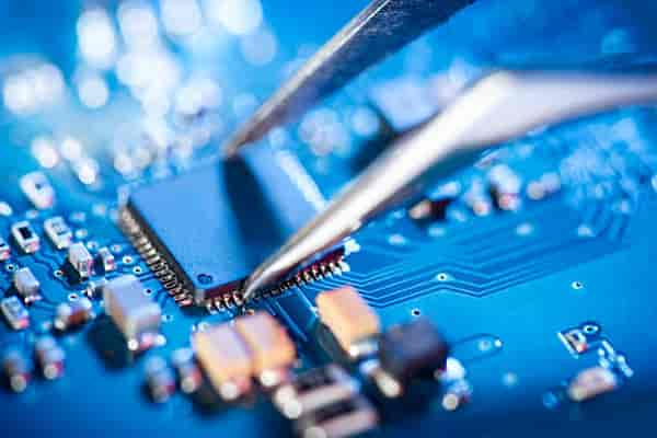
1.2 Solder Mask and PCB Assembly
- On the one hand, a solder mask is essential when it comes to fabricating your PCB. And the assembler will remind you that always put the solder mask dams between surface mount pads if possible, preventing accidental solder bridging as assembly and avoiding reworking required to remove shorts.
- On the other hand, a solder mask is also used to prevent solder starvation. For many reasons, it’s easy to be solder starvation; however, the mask can prevent solder from taking away from its intended location. Open vias near the surface mount pads (such as with BGAs) can clean up the solder and open the vias without connecting. What’s more, a mask is frequently used to tent or plug these vias to prevent this. You should know that you cover everything with a solder mask unless you need to solder to it or use it as a test point.
1.3 Compatibility with Surface Finishes and Assembly Processes
The selection of the appropriate solder mask for your PCB design must take into account its compatibility with various surface finishes and assembly processes. The solder mask’s interaction with these elements can significantly impact your PCB assembly’s reliability, performance, and long-term durability.
Interactions with Surface Finishes
Surface finishes, such as Hot Air Solder Leveling (HASL), Electroless Nickel Immersion Gold (ENIG), and Immersion Tin (ImSn), are applied to exposed copper areas on the PCB, including component pads and connector fingers. These finishes serve several purposes, including preventing oxidation, enhancing solderability, and improving electrical conductivity.
Ensuring that the solder mask material is compatible with the chosen surface finish is crucial. Incompatibility can lead to issues such as delamination, cracking, or poor adhesion, which can compromise the integrity of the PCB assembly and increase the risk of failures.
Solder Mask Compatibility with Reflow and Wave Soldering
The solder mask’s compatibility with various soldering processes, such as reflow soldering and wave soldering, is another critical consideration. During these processes, the solder mask is exposed to high temperatures and molten solder, which can potentially cause degradation or damage if the solder mask material is not suitable.
Reflow Soldering: In reflow soldering, the PCB and its components are subjected to a controlled temperature profile, causing the solder paste to melt and form secure electrical and mechanical connections. The solder mask must be able to withstand these high temperatures without degrading, cracking, or delaminating.
Wave Soldering: Wave soldering involves passing the PCB over a molten solder wave, allowing the solder to flow onto the component leads and pads. In this process, the solder mask plays a crucial role in preventing solder bridging and ensuring proper solder joint formation. The solder mask material must be resistant to elevated temperatures and direct contact with molten solder.
Compatibility with Other Assembly Processes
In addition to surface finishes and soldering processes, the solder mask’s compatibility with other assembly processes, such as conformal coating application, must also be considered. Conformal coatings are often applied to PCBs to provide additional protection against environmental factors, such as moisture, chemicals, and vibrations.
Ensuring that the solder mask material is compatible with the chosen conformal coating can prevent issues like delamination, cracking, or poor adhesion, which can compromise the overall protection and reliability of the PCB assembly.
By carefully evaluating the compatibility of the solder mask with various surface finishes, soldering processes, and other assembly steps, you can minimize the risk of failures and ensure the long-term performance and reliability of your PCB assembly. Consulting with your PCB manufacturer and adhering to industry standards and best practices can help you make informed decisions regarding solder mask selection and compatibility.
Recommended PCB Manufacturing Services


2. 4 Main Types of PCB Solder Mask
There are many PCB solder masks, such as Epoxy Liquid, Liquid Photoimageable, Dry Film Photoimageable, Top- and Bottom-side Masks.
2.1 Top- and Bottom-side Masks
A topside solder mask allows the electronic engineer to identify the openings in the green solder mask layer already added to the PCB by epoxy, ink, or film techniques. Component pins can then be soldered onto the board using those identified places. The conductive traces on the top side of the circuit board are called full traces, and the bottom-side mask specifies openings on the lower surface.
Multilayer circuit boards have three or more layers. Read the following article to learn more about the stacking information of multilayer PCBs:
2.2 Epoxy Liquid
Silkscreened onto the PCB pattern, the epoxy liquid is the lowest cost type of solder mask. Epoxy is a thermosetting polymer that has many applications. Silkscreening is a printing technique that uses a woven mesh to support ink-blocking stencils or patterns. The mesh creates open areas for ink transfer. Silk is often used in art, but synthetic fibers are more common for electronic applications. The final finishing process involves thermal curing.
2.3 Liquid Ink Photoimageable
Currently, the most commonly used solder mask is liquid photo imageable solder masks. There are several LPI methods: silk screen printing, curtain coating, electrostatic spray, and air spray.
A liquid photo imageable solder mask is delivered as an ink formulation. The ink can be silkscreened or sprayed onto the PCB, then exposed to the pattern and developed. One type of process commonly used with liquid ink formulations is hot air surface leveling (HASL). It requires a clean environment, free of particles and contaminants. After the UV light exposure stage, the mask is removed using high-pressure water sprays called developers. Circuit board finishing requires thermal curing and organic coating.
Since the introduction of Liquid Photo Imageable Solder Masks (LPI) in the late 1980s, it has continued to be applied on printed circuit boards, such as rigid PCB, rigid-flex PCB, and flexible PCBs. LPI solder mask is by far the most common type of solder resists used today. LPI is more reliable, can be printed very accurately, and makes better contact with the board’s surface and the copper features they’re applied to protect. LPI solder mask is an epoxy-based material, so it is very durable and nearly impossible to remove once cured. Various methods use LPISM ink, such as screen printing, curtain coating, electrostatic spray, air spray, etc.
Liquid Photo Imageable Solder Mask usually is applied to the printed circuit board in the following steps:
- The plate should be thoroughly cleaned to ensure no dust particles are trapped on the surface.
- The plates are completely covered on both sides with the liquid mask.
- The coated plates are placed in an oven to tack-dry the mask.
- A film is made of the solder mask Gerber files. The film will be transparent where you want to apply a mask to the board. Where the cover should be removed will be black on the film.
- The tack-dried boards are placed into a UV developer, and the film is precisely aligned over the board. The film’s black area will prevent the UV light from curing the mask where it is not wanted.
- After the mask is exposed to the UV lamps, and the uncured cover is washed off.
2.3.1 LPI Electrostatic Spray
Fundamental:
In the electrostatic spray technique, LPI is applied from a rotating bell, aided by compressed air, atomizes the ink, and deposits it on the PCB. The principle of Electrostatic Spraying is based upon the physics principle of “As charges repel. Unlike charges attract”. The LPI is given a negative charge, and the PCB is earthed, so the LPI is attracted to the board. The negative charge on each of the resist droplets helps to reduce droplet size further. However, despite the electrostatic attraction, there is some 10 – 20% loss of resistance due to overspray. And the electrostatic effect tends to attract the LPI to the copper areas, resulting in a less than perfectly uniform coating.
Electrostatic coating is a manufacturing process that employs charged particles to more efficiently paint a workpiece. In the form of either powdered particles or atomized liquid, Paint is initially projected towards a conductive workpiece, using standard spraying methods, and is then accelerated toward the workpiece by a powerful electrostatic charge.
Typical Powder Coating Process:
Pretreatment- Spray-Baking- Clean-Inspection-Package
Typical Powder Coating Equipment:
Powder room, high-voltage electrostatic generator, electrostatic spray gun, powder feeder, powder recovery, etc.
2.3.2 LPI air-spray
Using air spray, the LPI is applied using a single spray gun or multiple spray guns. This is a conventional spray technique where thin liquid resists are intermixed with decompressing air at the nozzle of a spray gun. The resulting atomized droplets resist and are then carried by the air pressure force onto the circuit board. Air spray generally produces a uniform coating with multiple gun spray systems tending to form “stripes” due to overlap or interference between adjacent guns across the board.
This application technique has been used for over 70 years but has only recently been introduced into the printed circuit market. Compared with electrostatic spray, the spraying principle of air spray is slightly different, and the equipment is less expensive. And the production rates, loss in overspray, and coverage over panels of electrostatic and air spray are similar. The kit is available to coat circuit boards horizontally or vertically.
2.3.3 LPI Curtain Coating
Curtain Coating – High-Speed with Low Material Loss LPI Applying Method
Curtain coating has become more widely used in the circuits industry as PCBs have become more complex, with higher track densities and narrower track widths. With the curtain-coat technique, LPI is applied as the printed circuit board passes through a sheet, or curtain, of low viscosity ink, falling through a narrow slot. The curtain coating can use liquid material at a very high speed with low material loss.
Curtain coating appears as a coating variation phenomenon – “shadowing.” Shadowing results from reduced solder mask on the trailing edge of traces parallel to the curtain compared with the leading edge of those traces.
2.3.4 LPI Silkscreen Printing
Silk Screen Printing,The Most Common Used LPI Solder mask Application Method.
Semi-automatic screen print-applied LPISM is the most commonly used solder mask application method today. The silkscreen process started to develop rapidly in about 1921. Now highly automated and has become established in a wide variety of decorative and industrial fields, including the printed circuit industry. Of all the available printing techniques, the screening process is well adapted to published circuit production requirements. Depending on the application, it can deposit resistance on both non-etched and etched boards over a wide range of film thicknesses.
The silkscreen printing applies the LPI to the circuit board with a squeegee blade through a tensioned mesh. Ink deposit is controlled by varying the mesh count and print settings, speed, angle, and pressure. A stencil-like image is supported on a fabric mesh stretched across a rectangular frame. During printing, the structure is supplied with ink, which is flooded over the screen. A squeegee is then drawn across it, with the ink flowing through the mesh’s open cells. Simultaneously, the substrate is held in contact with the screen, and the ink is thus transferred to it from the available sections of the mesh.
Non-uniformity of the coating can result from the damming effect on the leading edge of the trace in the squeegee movement’s direction. There is compression of the screen on the crown of the trace, resulting in a skinny coating, and the flooding effect in the space between the traces also must be taken into account. All affect the resulting impedance.
A working supply of ink is placed at one end of the screen. The screen is then lowered into position, and a rubber squeegee is drawn across the stencil to produce the print.
On most automatic flatbed machines, the base to which the substrate is applied is in a vacuum. This prevents the laminate from sticking to the screen when tacky inks are used.
2.4 Dry Film Photoimageable
Traditional printed circuit boards rarely use solder masks; however, the SMT circuit boards generally will use a solder mask. Solder mask is a polyethylene material, mainly divided into two types, dry film and wet film.
Dry film photoimageable solder mask is applied using vacuum lamination, then exposed and developed. After developing, openings are created in the pattern, and parts can be soldered to the copper pads. Copper is layered onto the board inside the holes and on the trace areas using electrochemical processing. Tin is applied to protect the copper circuitry. The dry film is then removed, and the exposed copper is etched. Finishing also involves thermal curing.
When the non-permanent solder mask is soldered in the wave, the wave will go through tooling holes in the circuit board to the non-welding surface. Therefore, before inserting components, the mounting holes and gold finger should be covered up with a non-permanent solder mask and then dissolved away during the cleaning.
A permanent solder mask is an integral part of the PCB board. It prevents the bridges from connecting while soldering in waves and protects the wiring from mechanical damage or chemical corrosion. A permanent solder mask is divided into dry and wet films. The dry film is water-based or solvent-based.
Dry film solder mask graphics have a high resolution, suitable for high-density wiring boards, and are accurately aligned. So it will not flow into the through holes in the circuit boards. When the circuit board is tested in a needle bed, the vacuum should be used to suck the board to locate. What’s more, the dry film is not easy to be polluted, so it will not affect the reliability of welding.
Some negative factors are using dry film:
There are pads and lines on the PCB boards’ surface, so the body is not smooth, and the dry film solder mask has no liquidity. So, there may be gas left between the dry film and the surface of the circuit board. The gas gets expanded when heated, which may cause dry film rupture phenomena.
The dry film is relatively thick. Generally, the thickness is 0.08 ~ 0.1mm (3 ~ 4mil). The dry film covering the surface of circuit boards may cause the offset phenomenon.
The curing conditions of dry film solder masks are stringent; if the curing temperature is too low or the curing time is too short, then the curing is insufficient. It will be affected by the solvent while cleaning. If the curing is too brittle, it may crack when exposed to heat stress. What’s more, dry film solders resist low thermal shock resistance, easy to get broken in high temperatures. The price of the dry film is increased than the wet film.
3. What is the Solder Mask Process?
The solder mask process involves plenty of steps. The general steps include:
- Pretreatment
- Coating
- Plughole
- Drying
- Pre-Baking
- Registration
- Exposure
- Developing
- Inspection
- Final Curing
- Final cleaning
- Pretreatment – clean
It is hard to combine the copper and solder layers if the copper surface is oxidized or too smooth. The weak combination cannot resist such as the thermal shock in the subsequent processes. To avoid this problem, there is a Pretreatment before coating. The oxidized layer should be degreased with the help of a pre-cleaning step. And the copper surface should be made rough to enhance the adhesion.
- Coating – Silkscreen
Coating, also called screen printing, is to apply the solder mask color according to customers’ requirements to the circuit board.
You’d better plug up the hole, which controls by the adjustment of the scraper.
The critical points of the printing process:
A: three-points bonding pressure: 6㎏/㎝2~8㎏/㎝2;
B: the scraper pressure: 4.5㎏/㎝2~6.5㎏/㎝2;
C: Scraper degree: 45°~90°;
D: printing speed: 8.5m /min~1.68m /min;
E: The thickness of ink: 15-25μm;
F: quiescence time: 15-20min.
- Plughole
With PCB technology development, more and more PCB manufacturers require to make the plughole with a solder mask for the vias. And the plug hole aims to prevent anti-solder flux from the via because it’s accessible to short circuit as wave soldering.
- Drying
After screen printing, the board should be dried at least for 15 minutes before pre-baking. It helps to reduce the load of the pre-baking by solvent evaporation.
- Pre-Baking
The purpose of pre-baking in a tunnel oven is to go on evaporating the ink solvent. Pre-baking temperature, time, and ventilation control are critical. The too high or too long pre-baking temperature will cause difficulty in developing.
- Registration
After pre-baking, there is a registration step with the film.
- Exposure
Would you please check whether the polyester film and glass frame in the exposure frame is clean or not before exposure? Then turn on the exposure machine’s power switch and open the vacuum button to select the exposure program. Before the proper direction, the exposure machine should work in vain five times to lead the exposure machine to enter the best working state. The exposed areas will be remained, while the unexposed areas will be washed out.
- Developing
Developing is to remove the solder solvent on the pads in some shading parts. The development solution is 1% Na2CO3. The liquid temperature is usually around 28 to 32 degrees Celsius. Before the formal development, you should improve the developing machine’s climate, and the solution can reach the predetermined temperature to achieve the best developing effect.
- Inspection
After the developing step, inspection is needed to check whether there is any defect image, and the burrs should be removed. Please pay attention to wearing yarn gloves and holding the sides of the boards in the inspection process.
- Final Curing
Put the qualified circuit boards into the tunnel oven for baking for the final thermal curing. Sometimes, additional UV curing will be needed to increase the solder mask’s chemical and mechanical properties.
- Final cleaning
The boards are covered with solder masks, which need to be cleaned up before further processing, such as surface finish, assembly, and so on.
Learn More About PCB Manufacturing Process
4. The Main Types of Solder Mask Ink
Thanks to the rapid development of the PCB industry, PCB ink manufacturers obtain more chances.
PCB solder resists ink industry is of high-tech. It involves paint and ink manufacturing technology, ultra-fine powder application technology, UV curing technology, lithography technology. Some products must require a high temperature above 280 ℃ resistance weldability, line precision performance to 25 microns, chemical nickel plating, tin resistance, above 1011 ohms electrical insulating properties, high voltage above 20kV breakdown performance, UV sensing optical properties.
PCB ink needs to be low-toxic, odorless, safe, and environment-friendly to reduce environmental pollution and harm to the operators. Some solder mask ink manufacturers and experts have already started to develop non-toxic solvents. Many ink buyers from different countries have begun to purchase solder resist from China’s PCB ink manufacturers, which indicates that China’s PCB ink has also occupied a specific international market. More chances mean more challenges. It improves China’s PCB ink manufacturing technology, leading to related technologies and other associated products.
The commonly used solder resist ink is :
- Thermal Curing Solder Resist Ink
- UV Curing Solder Resist Ink
- LPI Solder Mask Ink
The screen printing process conditions of UV curing solder resist ink is the same as the resist printing ink.
Compared with thermal curing solder resist ink, UV curable solder resist ink has many advantages, such as no solvent, low volatility, low toxicity, environment-friendly, fast-drying, adapting to automated or semi-automated assembly line operations. The most significant advantage is that the curing temperature is low, with no thermal reaction for the laminate, and does not change the substrate size or cause a warping phenomenon. However, the thermal curing solder resists ink has better adhesion and heat resistance on the substrate than UV curing. So before UV curing, there should be a stricter pre-cleaning.
Whether thermal curing solder resist ink or UV curing solder resists the ink, it can only be used for single-sided PCB and low-end electronic products. The applying method is screen printing. With the circuit and the pad graphic line spacing becoming much denser, the original graphic screen printing method has not met the solder resist layer’s printing requirements.
Although the dry film solder method has been popular for a few years, the manufacturing technology is not widely spread because of its expensive materials. The operation process is complex low yield, so this technology has now been substantially eliminated. Currently, the LPI solder mask ink is used for a high-density, high-precision printed circuit board. It has been gradually showing its advantages in high-end PCB.
5. 10 Characteristics of PCB Solder Mask Ink
Ten characteristics of PCB solder mask ink is
- Viscosity
- Plasticity
- Thixotropy
- Fluidity
- Viscoelastic
- Dry
- Fineness
- Stringiness
- Transparency and Opacity
- Safe and Environment-friendly
Viscosity
Viscosity is short for dynamic viscosity. It equals the shear stress/velocity gradient. Its international unit is Pa / sec (Pa.S) or mPa / sec (mPa.S). In PCB production, it means the fluidity of ink is driven by external forces.
Plasticity
Plasticity means that after the deformation is driven by external forces, the ink could retain the properties as before. Ink plasticity will help improve printing precision.
Thixotropy
Thixotropic, also known as rock degeneration, sag resistance, is a physical characteristic of a liquid. Its viscosity declines under stirring, but it will recovery its original thickness at a standstill very fast. By stirring, the thixotropic effect lasts for such a long time that the ink could re-constitute the internal structure. The solder mask ink becomes liquid when it is gone. This accelerates the speed of ink through the screen mesh and promotes the ink evenly fused.
Fluidity
Leveling is the ink expansion degree to the surrounding, driven by an external force. Fluidity is the reciprocal of viscosity. Fluidity is related to ink plasticity and thixotropic.
Viscoelastic
Viscoelastic refers to the ink squeegee blade after being shear fracture ink quickly rebound performance. Requirements deformation speed ink, the ink can rebound rapidly in favor of printing.
Dry
The slower the ink gets dried on the screen, the better. But the faster the ink gets dried, the better when the solder mask is transferred to the substrate.
Fineness
Fineness is the size of Pigment and solid particles. PCB ink size is generally less than 10μm; the fineness should be less than one-third of the mesh opening.
Stringiness
When the ink shovel stirs the ink, filamentous ink will not be torn, called stringiness.
Transparency and Opacity
For PCB ink, different requirements for transparency and opacity of inks are needed according to further usage. In general, circuit ink, conductive ink, and legend ink require high opacity. The solder resists more flexibly.
Safe and Environment-friendly
PCB ink requires low-toxic, odorless, safe, and environment-friendly.
6. Solder Mask Thickness
When it comes to solder mask selection, thickness is a critical parameter that can significantly impact the performance and reliability of your PCB assembly. The appropriate solder mask thickness depends on various factors, including trace widths, component pad sizes, and clearance requirements. Let’s explore the importance of solder mask thickness and the typical ranges used in PCB manufacturing.
Typical Solder Mask Thickness Ranges
The thickness of the solder mask is usually measured in micrometers (μm) or mils (1 mil = 25.4 μm). In general, the solder mask thickness ranges from 15 μm (0.6 mils) to 35 μm (1.4 mils), with the most common values being between 20 μm (0.8 mils) and 25 μm (1.0 mil).
Relationship between Trace Width and Solder Mask Thickness
The width of the copper traces on your PCB design plays a crucial role in determining the optimal solder mask thickness. As a general guideline, the solder mask thickness should be approximately half the width of the narrowest trace on your board. This ensures that the solder mask provides adequate coverage and protection for the traces while minimizing the risk of solder bridging or other defects.
For example, if your PCB design has traces as narrow as 100 μm (4 mils), a solder mask thickness of around 50 μm (2 mils) may be appropriate. Conversely, if your design features wider traces, a thicker solder mask may be used to provide better coverage and protection.
Solder Mask Tenting and Clearance Requirements
Another important consideration related to solder mask thickness is the tenting requirements for component pads and vias. Solder mask tenting refers to the process of creating a small opening or “tent” in the solder mask over a pad or via, allowing access for solder paste or wire bonding.
The thickness of the solder mask plays a crucial role in determining the size and shape of these tents. Thicker solder masks may require larger tent openings to ensure proper solder flow and joint formation, while thinner solder masks allow for smaller and more precise tent openings, which is particularly important for fine-pitch components and high-density interconnects.
Additionally, the clearance between the solder mask and component pads or other features must be carefully considered. Insufficient clearance can lead to solder bridging or other defects, while excessive clearance may compromise the insulation and protection provided by the solder mask.
By carefully evaluating your PCB design requirements, trace widths, component pad sizes, and manufacturing processes, you can determine the optimal solder mask thickness that balances performance, reliability, and manufacturability. Consulting with your PCB manufacturer or design experts can also provide valuable guidance in selecting the appropriate solder mask thickness for your specific application.
What’s the impact of the solder mask thickness?
If the solder mask is too thin, the copper will be exposed, causing SMT problems. According to IPC standards, the corner lines are usually greater than 8 microns. Otherwise, it will be yellow while baking and will result in leaking copper.
If the solder mask is too thick, the parts may appear tilt, affecting welding quality, resulting in IC Weld and other issues. Heavy copper always has thick solder resistance.
It is not very easy to scratch once we use a squeegee blade to scrape the solder mask on the copper’s surface. Besides, a good solder mask cannot be easily worn because of its excellent adhesion strength. Only when someone in the production line scrapes the solder resist with a sharp metal blade deliberately; otherwise, even if the thickness is slightly thinner, the copper will also be not seriously exposed. What the most important is whether the solder mask adhesion strength is enough or not.
Therefore, most customers will limit the upper limit of the ink. According to the visual inspection standard, the lower limit will not be strictly controlled as long as the copper is not exposed (including pseudo exposed copper).
If you want to inspect the solder mask thickness, you can take some slices of the printed circuit board to measure the solder resist thickness at different locations on the circuit.
7. What is Peelable Solder Mask?
Peelable Solder mask (PSM) PCB is the printed circuit board with peelable solder mask (a temporary solder mask), protected for some area during surface finishing or assembly. That’s to say, sometimes printed circuit boards require protection of selected board areas during the Surface Finish or Assembly Process to keep solder from flowing onto contacts, terminals, and plated through holes (PTH).
Peelable mask, also as strippable mask or blue mask, is applied to the already solder mask PCB to protect circuit by screen printing. Peelable Solder Masks protect soldering processes like wave soldering, reflow soldering, or hot-air solder leveling (HASL).
When these processes are over and the solder mask is no longer needed, it can be mechanically removed or “peeled-off” by hand. The area is used to protect the exposed for the final assembly process. A peelable mask is not a replacement for standard solder resistance.
The Advantages of peelable solder mask:
- Reliable, time & cost saving
- Protect shapes by screen-printing
- Protect selected areas on PCB
- Easy removal and no residue
- Stable to high temperature
8. Solder Mask Misregistration
Surface Mount Technology (SMT) needs smaller, higher input/output components for new electronics applications, which requires reduced size and higher density interconnect for new area array packages. However, there are still many challenges for assembly, including solder short prevention and detection.
Some process issues can be caused by solder mask misregistration that occurred at PCB fabrication. Solder mask misregistration may result in problems with exposed adjacent traces and/or vias underneath array packages, increasing shorts’ opportunity. Solder bridging could have formed during the solder paste screen printing process when an adjoining trace is exposed due to solder mask misregistration. The acceptable solder mask registration criteria must be much stricter than standard PCB solder mask fabrication requirements.
Solder mask Registration for Pad-to-Trace separation needs to be taken into account. Considering solder mask registration, the openings should extend 3mils beyond the copper on pads. In this way, if there are 3mils of registration error between the mask and the copper, there will also be no solder mask on the pad. This is very important because solder resistance on the pad may cause assembly defects. The solder mask opening is usually 3mils, adding up the 3mils solder mask registration tolerance, so it means the minimum pad-to-trace gap must be six mils.
To ensure the solder mask registration, the following can be noticed:
(1) For accurate film alignment, the film’s expansion and shrinkage should be precisely measured.
(2) The recommended temperature of the no-dust room is 18-22 °C, the recommended range of humidity is 45-65% to ensure the film’s stability.
(3) When many boards are in production, the film needs a protective layer to prevent film rubbing, resulting in ink residue.
9. Solder Mask Expansion
A solder mask is a protective layer for PCB boards. But the pads for components assembling on the circuit boards cannot be covered with solder mask ink. These pads part should avoid applying the solder mask.
Solder mask Expansion – the value applied to the initial pad/via shape to obtain the final form on the solder mask layer. Please enter a positive value to expand the initial pad/via shape; enter a negative value to contract it. It is the extended distance between SMT pads and the solder mask layer. In producing a printed circuit board, there should be some space for pads on the solder mask layer, which avoids overlapping the solder mask layer and pads. With PCB designs, you need to ensure that the solder mask is never on top of SMD pads. The solder mask expansion standard is 4mil.
In practice, things never align perfectly. The actual holes punched in the solder mask may be slightly less than what you specified (“shrinkage”), and the holes are always be placed in a slightly different location than what you selected (“movement”). Suppose the solder mask expansion is too small. In that case, these misalignments cause the solder mask to partially or entirely overlap SMT pads and through-hole pads, perhaps causing the uneven placement of the components on the board. If the pads are covered with the solder mask, the SMT part will be disconnected. If the solder mask expansion is too significant, it won’t prevent neighboring pads from bridging during soldering.
10. How to Test PCB Solder Mask?
We know that solder mask is widely used on printed circuit boards. After the solder mask process, sometimes you need to inspect whether there is any problem with solder resistance.
- Solder quality test: direct visual inspections and then with 1.5 to 10 times magnifier.
- Adhesion (tape test): According to IPC-TM-650 / TM2.4.28.1 Standard, testing peel strength by 3M tape.
- Hardness Test: According to IPC-SM-840C 3.5.1 / TM 2.4.27.2 Standard, draw an inch long line on a board after the baking with a pencil hardness (JIS standard) and use about one Newton force at an angle of 45 ℃. Use an eraser to remove the toner and check whether there are scratches. It is ok when the copper is not exposed.
- Acid and alkali resistance test: according to IPC-SM-840C 3.6.1.1 standard, take two 6PNL silver test panels of each dipped into 10% HCl, 10% H2SO4, 10% NaOH solution for 30 mins. Then take another two 6PNL OSP panels immersed in 10% HCl, 10% H2SO4, 10% NaOH solution for 60mins. Then inspect whether the surface blistering, peeling, discoloration, and other situations occur.
- Solvent resistance: according to IPC-SM-840C 3.6.1.1 standard, clean coating surface, inspect whether the surface blistering, peeling, discoloration, and other situations occur.
- High-temperature resistance
1)Welding: according to IPC-SM-840C 3.7 standard
2)Soldering resistance: according to IPC-SM-840C 3.7.2 standard
3)Solder heat resistance
4)Tin drift test: Temperature: 260 ℃, time 10S, the test three times - Solder mask ink thickness: take silver and OSP board to do several sections, measure the ink thickness at different locations.
- Undercut: To measure whether the deepness of the undercut is within 1.2mil.
- Thermal shock resistance: According to IPC-SM-840C 3.9.3/TM2.6.7.1 standard, H degree, 65~125°C,100times cycling,inspect whether the surface blistering, peeling, discoloration.
- Solder Dam Test
Design 2mil, 3mil, 4mil, 5mil solder dam on the negative film (according to the various process capabilities). After development, baking, FQC, check whether it is off.
11. The Common Problems and Solutions of PCB Solder Mask
According to some percentage, the solder mask for printed circuit board printing is mixed with ink and curing agent. The two materials should be thoroughly mixed and then stand for 30min-45min. The solder mask cannot be used until it is cured. The hybrid ink viscosity is about 150 + 20PS (25℃). The viscosity of the mixture decreases with the increase of temperature.
We will refer to the common problems and troubleshooting faults for using the solder resist to guarantee the PCB Board manufacture.
Problems:
- Solder resist ink is not even attached to the plate surface
- Mixing time for solder mask ink is not enough
- Ink mixing faults
- There is residual grease or water stains on the plate surface (incomplete pre-treatment)
- Ink impurities (grease dropped in and destroyed the surface tension)
- Bad scraping film material
- Dirty Screen
- Use expired ink
Solutions:
- Guarantee a complete pre-treatment
- Check water breaking, grinding marks, etc. meet the standards
- Make sure the ink mixing parameters
- Clean the screen, replace squeegee blade and other tools
Problems:
- Ink and copper surface are separated
- Inadequate pre-treatment
- Impurities attach to the plate surface
- Copper surface depression
- Adverse ink mixing
- Uneven thickness of the ink on the copper surface
- Damage on the ink surface
- Variable oven temperature and baking inadequate or over-baking
- Multiple HAL or HAL temperature is too high
Solutions:
- Guarantee a complete pre-treatment
- Make sure the oven baking temperature and the heating curve distribution
- Make sure the ink mixing parameters
- Check the production process to reduce the external impact
- Confirm HAL operating parameters and status
Problems:
- Ink overflow after exposure
- Bad exposure
- Orientation film not in the hole
- Vacuum pressure instability
- Debris attached to the negatives film
Solutions:
- While exposure, attach the film to the board
- Use thinner strips than plates
- Location PIN needs to insert into the positioning hole
- Check the negatives film
Problems:
- Ink overflow after baking
- No section of the warming
- The temperature is too high for the low-temperature section
- The time is too short for the low-temperature section
- The low-temperature section is not continuously baked
- Oven temperature is uneven
Solutions:
- Continuous baking
- Confirm the oven temperature
- Hot air must be in the same direction
- Confirm the parameters
12. Solder Mask Bridge Breaking Off Pads
Reasons for Solder Mask Bridge Breaking Off
The solder resists between the SMD pads are called the solder mask bridge (solder mask dam), which prevents bridging and short circuit when welding. Sometimes the solder mask bridge breaking off happens in many printed circuit board companies, affecting product quality and production efficiency. With the rapid development of the PCB industry, the requirements of customers are getting higher and higher. It is time to improve the processing capacity of the solder resist bridge. What are the factors affecting the solder mask bridge breaking off?
The main reason for the solder mask bridge breaking off is that UV intensity decreases rapidly with the transmission depth of solder mask ink. When the ink is more than a specific thickness, it will not be fully photo-polymerized, so undercut, and solder mask bridge breaking off happen when developing. Meantime, the exposure energy, developing time, precure time, and so on will influence breaking off the solder mask bridge.
- Exposure Energy
With the increase of the thickness of the solder resist under the same exposure degree, the solder resists bridge’s undercut increases. The solder mask bridge breaking off also appears, and the solder mask bridge production capacity decreases. When exposed to ultraviolet light, part of the UV is absorbed by the liquid photosensitive solder resist ink. Due to the absorption, the intensity of UV decreases gradually, so when the UV light reaches the bottom of the ink, its energy is very weak. Therefore, when the ink comes to a certain thickness, the resin’s bottom will not be incomplete photo-polymerization status, resulting in undercut while developing.
When the bottom ink is not fully photo-polymerized, increasing the exposure energy can result in better photo-polymerization of the bottom ink, so that undercut reduces. But it isn’t easy to eliminate. And in the actual production of the PCB circuit boards, the exposure energy cannot be unlimited increased.
- Developing Time
When the solder mask is not thick, such as 25-50um, the developing time has less impact on the undercut of the solder mask bridge; When the solder mask is thick, such as 70-75um, the developing time has more effect on the undercut of the solder mask bridge. With the decrease of developing time, the undercut of the solder resists decreases obviously.
- Precure Time
When the solder mask is not thick, such as 25-50um, the precure time has less impact on the undercut of the solder mask bridge; When the solder mask is thick, such as 80-85um, the precure time has more effect on the undercut of the solder mask bridge. With the increase of precure time, the solder resists’ width increases, so the undercut decreases.
- Other Factors
Other factors, such as precure temperature, developing pressure, developer potency, and developing temperature, will also influence the undercut and solder mask bridge breaking off.
Conclusions:
- When the ink reaches a specific thickness, it will not be fully photo-polymerized because the intensity of UV decreases rapidly with the transmission depth of solder mask ink, so undercut. Solder mask bridge breaking off happens when developing.
- Increase exposure energy can reduce undercut.
- Developing Time, precure time, precure temperature, developing pressure, developer potency, and developing temperature will also influence the undercut and solder mask bridge breaking off.
13. What Are The Possible Reasons for The Solder Resist Color Differences?
Is there some time when you receive your printed circuit board, the solder mask color is not what you want or expect? What are the possible reasons for the solder resist color differences?
Many things could cause color differences.
- Since the solder mask is a mixture of two parts, having too much of one or the other can cause variance in color. There is never a 100% guarantee that the color will be the same every time.
- There may be a shade difference.
- Material color could come in lighter or darker, affecting the look and color of the solder mask.
- Most Customers have no explicit mention of their requirement towards mask color in PCB Gerber / PCB drawing. That’s to say; the color is not clearly defined as light or dark in matte or semi-gloss or gloss finish.
- Solder mask colors may differ from different manufacturers or brands.
- Copper from outer layers can cause color differences; if the outer layer has extensive copper plains, they will look different in color than a board with outer layers that have less copper showing.
- Hot air level machines have also been known to change the mask’s color due to the stress of the process.
14. What are the Differences Between Solder Mask and Paste Mask?
Many beginners may be confused about Solder Mask Layer and Paste Mask Layer because they have some similarities. This article will introduce the differences between solder masks and paste masks so that beginners can understand better.
The solder mask is the layer, except the pad (surface pads mount pads, plug-in pads, vias) on PCB boards; the other areas should be covered with the solder resist ink. These pads are exposed to avoid tin during wave soldering. It is also usually called the solder mask layer or green layer.
The solder mask layer can be divided into Top Layers and Bottom Layers. The small circles or small square circles in the Gerber file are the holes on the solder mask for exposed pads, generally more significant than the pad.
The paste mask layer is generally called a stencil in the industry. Generally, the hollow shape size is the same with SMD pads or slightly smaller. This stencil is used in the SMD automatic assembly soldering process to coat the SMD pads with tin paste. In the surface mount device (SMD) welding process, first, cover the stencil to the circuit board (aligned with the corresponding pads), and then apply the paste, remove the excess paste with a blade, next take away the stencil so that the solder pads are used with paste. Afterward, attach components to the solder paste (by hand or assembly machine), and finally through the reflow soldering machine to complete the SMD assembly. Usually, the stencil sizes will be smaller than the actual welding pads on the circuit board. The paste mask layer can also be divided into Top Paste and Bottom Paste.
Here are some differences between the solder mask and paste mask:
- The openings on the solder mask layer have no solder mask ink, but the openings on the paste mask layer have a paste.
- The solder mask layer is one part of the circuit board, but the paste mask layer is not. The paste mask layer is just for the stencil.
- A solder mask is used to apply solder mask ink, but a paste mask is used to apply the paste.
- Solder mask is applied when making a PCB board, but the paste mask is used when assembling.
- Solder mask has many available colors, but the paste mask is usually gray.
15. How to Repair the Solder Mask?
Generally, the solder mask is not comfortable to drop off after curing. The solder resists itself as a protective layer for printed circuit boards. If there is solder mask damage on a PCB, there are several methods to repair it.
You can use a dedicated solder mask repair pen to apply the ink to the circuit board. And then make it dry in an oven. If the PCB board is not assembled, you can bake it at a temperature of 150 degrees for 20-30 minutes. If it has already been assembled, you can bake it at the temperature of 120 degrees for about half an hour. It dries quickly in the oven. The repair pen is usually simple to use, and the ink mask is durable.
You can use something like an oily color pen to repair the board if it is just for aesthetic purposes. But this can only serve to temporarily improve the appearance, no insulation, and protection effects.
The BGA solder mask repair steps can be summarized as the following:
- Clean the area to ensure enough adhesion, optimize electrical properties, and minimize corrosive effects.
- Remove all of the extra solders from the BGA pads.
- Scrape or grind.
- Prepare the replacement solder mask material.
- Apply the coating replacement mask material.
- Let the epoxy cure in an oven.
- Confirm that the repair is completed correctly by checking the vias’ electrical continuity and the BGA pads.
16. How to Remove Solder Mask from Printed Circuit Boards?
It sometimes happens that some parts are covered with solder masks, where no solder resist is needed, such as testing points, grounding pads, and assembly pins. However, it does not mean that these boards are useless. There are several safe and reliable methods to remove the extra solder mask: scraping, milling, micro-grinding, and chemical stripping. These most commonly used methods have both advantages and disadvantages. This article will have a simple comparison of these methods.
- Scraping
Scraping doesn’t require unique technology or select settings, but it’s a noisy method. Generally, a skilled technician can remove the solder mask from unwanted areas with a knife, scraper, or chisel. However, if the unwanted areas are large, the operator will feel tired. So it is commonly used for the removal of the thin solder mask layer. This method can be used with other ways to clear the solder mask in the last step.
- Milling
Have you ever used a milling machine to remove the solder mask? It seems extreme, but it is a very efficient and accurate method for removing solder masks. Because of using a sharp cutter, the accuracy must be controlled. The milling system should be equipped with a microscope for visual assistance. Carbide vertical milling cutter is the most commonly used tool because it is sharp and can quickly enter the coating and reach the board’s surface. The opposite direction to turn round cutters effectively controls the depth, and the skills and experience are critical.
- Micro-grinding
This is the best technology for removing solder masks in a large unwanted area on the circuit board. In the market, there are several small desktop systems to remove the solder resist. Using a pencil-like handpiece, abrasive material will be moved forward. The abrasive material rubs the solder mask layer. The primary step of this process is friction, and thus will produce an electrostatic charge. The micro-grinding system must eliminate potential electrostatic damage if the circuit boards are equipped with electrostatic sensitive devices. To remove the abrasive material on the circuit board, it must be thoroughly cleaned.
- Chemical Stripping
This method is the most effective way to remove the solder resist on the copper surface. The stripping area should be isolated to the other parts of the circuit board surface. And then, apply the chemical stripping agent with a brush or cotton swab. Since the stripping agent is liquid, it is often difficult to control. The chemical agent will erode and decompose the solder mask. A chemical stripping agent generally comprising dichloromethane is a potent solvent. Dichloromethane can quickly remove the solder mask; if the delay time is too long, it will also erode the substrate. For these reasons, the chemical stripping agent must be very carefully used.
17. Factors Influencing Solder Mask Selection
Choosing the right solder mask for your PCB design is a critical decision that can significantly impact the overall performance, reliability, and manufacturability of your product. Several key factors need to be considered when selecting the appropriate solder mask type and specifications. Let’s explore these factors in detail.
Board Complexity and Surface Features
The complexity of your PCB design, including the density of components, trace widths, and surface features, plays a crucial role in determining the most suitable solder mask option. Boards with intricate layouts, high component densities, and fine-pitch components often require the precision and tight tolerances offered by photoimageable solder masks (LPSM or DFSM).
On the other hand, simpler designs with larger features and lower component densities may be better suited for more cost-effective options, such as liquid epoxy solder masks applied through screen printing.
Component Density and Clearance Requirements
The spacing between components and the clearance requirements for solder mask openings (often referred to as solder mask defined pads) are essential considerations. Boards with high-density interconnects, such as ball grid arrays (BGAs) or chip-scale packages (CSPs), demand precise solder mask patterning to prevent solder bridging and ensure proper solder joint formation.
In such cases, photoimageable solder masks (LPSM or DFSM) are often the preferred choice, as they offer superior edge definition and tighter tolerances compared to screen-printed solder masks.
Manufacturing Capabilities and Processes
The solder mask selection process should also consider the manufacturing capabilities and processes employed by your contract manufacturer or in-house production facilities. Different solder mask types may require specific equipment, materials, and expertise, which can influence their suitability and cost-effectiveness for your project.
For example, if your manufacturer has limited photoimaging capabilities, opting for a liquid epoxy solder mask applied through screen printing may be a more practical choice, despite potential limitations in precision or feature size.
Cost Considerations
While performance and reliability are paramount, cost is often a significant factor in solder mask selection, especially for high-volume or cost-sensitive applications. Liquid epoxy solder masks applied through screen printing tend to be the most cost-effective option, while photoimageable solder masks (LPSM or DFSM) typically involve higher material and processing costs.
However, it’s essential to balance cost considerations with the potential risks and consequences of using a lower-cost solder mask that may not meet the performance or reliability requirements of your application.
By carefully evaluating these factors and consulting with your PCB manufacturer or design experts, you can make an informed decision on the most appropriate solder mask type and specifications for your specific project requirements.
JHYPCB’s PCB Solder Mask Options
Printed circuit board solder mask options from JHYPCB are designed to meet your industry needs. We focus primarily on the technical nature of your PCB — such as elements like controlled impedance — and allow your team to make the PCB mask choice based on what you feel is most pleasing for your application.
Our production engineers have worked with almost every PCB color and finish option available and can ensure your PCB is printed just the way you like. Speak with a representative today to learn more about liquid photo imagable solder mask colors that might be preferred in your industry or that could help you stand out during your next demonstration.
Related Videos
How to Solder Mask PCBs by hands?
UV Solder Mask VS. Dynamask – a how to guide!
How to make a PCB prototyping with UV soldermask – STEP by STEP
FAQ
Most frequent questions and answers
The harm of PCB solder mask ink to the human body is not apparent, but if the person engaged in this work exceeds five years, it may cause some health risks. In addition, the ink has a pungent odor, which may hurt the nose and taste buds.
The solder mask ink is thick and thick before use, and thinner is needed when using it. It should not be directly contacted with the skin because it is corrosive. The ingredients of banana oil are benzene and esters, most of which are toxic and have carcinogenic chemicals.
The main reasons for the solder mask falling off in the PCB are:
1. The solder mask process is unqualified;
2. The quality of solder mask ink is not up to standard;
3. The temperature of the tin furnace is unreasonable, and the temperature is too high;
4. The thickness of the solder mask is not enough and is too thin;
5. The solder mask has an angle on the edge of the circuit;
6. There are bubbles in the solder mask process;
7. The curing process is not up to standard.
Solder mask bridge: It is the solder mask layer between two patches or IC pins. Because it is relatively long and narrow, it is called a solder mask bridge.
Solder mask clearance: Any place where there is no solder mask can be called solder mask clearance. The pads cannot be treated with a solder mask.
The printed circuit board is composed of pads, vias, solder masks, and silkscreen legend. The main functions of the solder mask in the PCB are:
1. The solder mask can effectively achieve the effect of insulation;
2. Protect the circuit; if there is no solder mask, the exposed metal circuit will be oxidized, and it is straightforward to cause a short circuit due to external factors;
3. Beautify the appearance;
4. Prevent the overflowing tin in the soldering process from causing a short circuit in the circuit;
5. During wave soldering, it can prevent non-soldering points from being contaminated by tin.
1. There is no solder mask ink for the openings on the solder mask; however, the paste is on the openings of solder paste.
2. Solder mask is part of PCB, but the solder paste is not, as solder paste is only for the SMT stencil.
3. Solder mask is used for solder mask ink, while solder paste is used for paste.
4. Solder mask is applied as fabricating your circuit board. However, solder paste is used for SMT PCB assembly.
5. There are so many available colors for solder masks, while solder paste is usually gray.
Related Posts
- Custom PCB Manufacturer In China
- Quick Turn PCB Manufacturer In China
- How To Search for a Reliable PCB Manufacturer
- Classification Of PCB Materials And How To Choose The Correct PCB Substrate
- What factors determine the price of PCB?
- How to store PCB boards?
- 10 Types of PCB Surface Finishes: All You Need to Know
- IPC Standards: A Guide to Standards for PCB Manufacturing and Assembly