PCB SMT Solder paste Stencils

What is PCB Stencil? PCB Stencil is made of stainless steel sheets by laser cutting process. It is instrumental for SMT or surface-mount technology PCB assembly, especially in component placement. PCB stencils make solder paste printing easier, faster, and more precise by ensuring that every pad receives a suitable quantity.

What is PCB Stencil or SMT Stencil?

PCB Stencil, SMT Stencil, SMD Stencil, Laser-Cut Stencil, Solder Paste Stencil, What is it?

PCB Stencils, also called SMT stencils or SMD stencils, are crucial in transferring the correct amount of solder paste to the right positions on bare circuit boards ready for PCB assembly. In other words, stencils can fast and efficiently ensure the most precise solder paste amount and optimal electrical connection. With solder stencils, it is possible to use solder paste printing machines to apply solder paste easily over the pads on PCBs.

  • Made of stainless steel sheet
  • For solder paste printing
  • Framed or frameless
  • We manufacture various PCB stencils that can fit all solder-paste printers or applications.

Detailed Introduction Of PCB Stencil

What is the use of PCB stencil?

Why SMT Stencils Are Important?

Solder Paste Printing

The PCB stencil serves two primary functions. The first is to ensure the precise placement of a material on a substrate, such as a solder paste, flux, or encapsulant. The second is to provide the formation of appropriately sized and shaped deposits.

Solder Paste Printing

Surface Mount Technology is an area of electronic assembly used to mount electronic components to the printed circuit board’s surface (PCB) instead of inserting components through holes as with conventional assembly.

The first machine to set up in the assembly process is the solder paste printer, designed to apply solder paste using a stencil and squeegees to the appropriate pads on the PCB. This is the most widely used method for applying solder paste.

Keeping control of this process is critical as any printing defects, if undetected, will lead to defects further down the line. With assemblies becoming more complex, the stencil’s design (Click here to download the IPC-7525 Stencil Design Guidelines) is critical, and care must be taken to ensure a repeatable and stable process.

Why do you need SMT STENCIL?

In electronics manufacturing, a solder paste stencil is used for the following reasons:

  1. When using SMT (Surface Mount Technology) in the design of the printed circuit board (PCB).
  2. When using automated component placement equipment (unless it is a hand-loaded prototype).

This equipment replaces the process of hand soldering each component. Once components are placed onto the solder paste covering the printed circuit board, the PCB is then heated or ‘baked’ to solder the components to the board.

How can you make sure you apply the solder paste with precision exactly where it needs to go?

SMT stencils, or surface mount technology stencils, are the answer. SMT stencils are the medium you use to transfer that solder paste onto the PCB.

Can you apply soldering paste without an SMT stencil?

Yes, but because of the precision required, trying to apply soldering paste everywhere it needs to go on the board by hand can be an extremely time-consuming, painstaking process. Furthermore, you cannot get the consistency when applying soldering paste by hand that you will get using a single SMT stencil. It’s important to consider that the chances of error are much greater when applying soldering paste by hand.

When applying soldering paste by hand, or trying to apply it without a perfect stencil you could face some very serious problems, like:

  • Short circuits
  • Voids in the soldering process
  • The desired printed result requires:
  • Smooth and burr-free side walls of the apertures
  • Flat, unstressed material
  • Uniform tension distribution over the entire surface
  • Precision in position and size of the apertures
SMT Stencil

How to use PCB stencil?

Squeegee solder paste through the stencil. The stencil ensures the solder paste is in the right amount in the correct position. Then you can place surface mount components on solder paste and put it into a reflow oven.

Play Video about How to use PCB Stencil
The Components of the SMT Stencil

Components and structure of PCB Stencil

Solder Paste

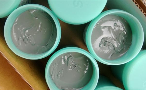
Step1: Preparation of solder paste

1. When the solder paste is not opened, it should be stored in a constant temperature and humidity freezer;

2. The temperature of solder paste needs to be consistent with room temperature before use;

3. The solder paste needs to be stirred before use, and the stirring time is about 3-5 minutes.

Soldering Paste Printing with SMT Stencil

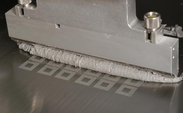
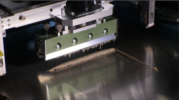
Step2: Solder Paste Printing

1. The temperature and humidity requirements of the solder paste in the printing machine: 25±3℃, RH 40~70%;

2. Scraper pressure: the edge of the solder joint is clear, the surface is flat, and the thickness is appropriate;

3. Scraper speed: ensure that the solder paste is rolling rather than sliding relative to the squeegee. In general, 10-20mm/s is appropriate.
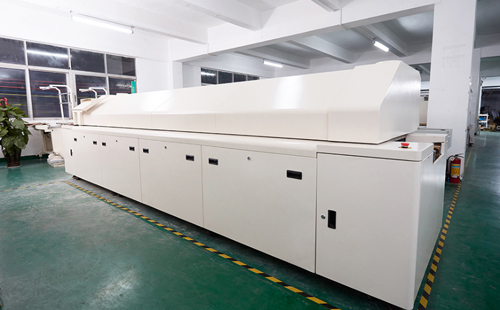
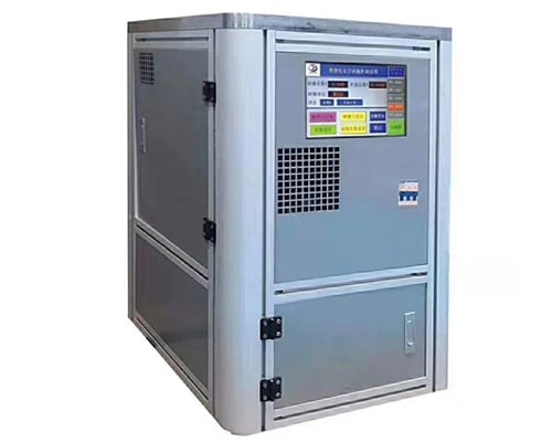
Reflow Oven

Step3: Reflow Oven

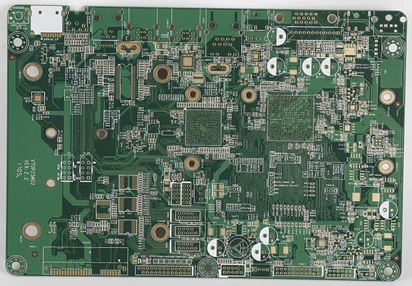
1. Reflow soldering can process surface-mounted circuit boards. The process is complicated and can be divided into single-sided PCB Assembly and double-sided PCB Assembly.

2. The reflow oven has at least 3 temperature zones: preheating, soldering, and cooling.

3. The difference between wave soldering and reflow soldering is that wave soldering is mainly used for soldering plug-ins; reflow soldering is used mainly for soldering SMD components.

SMT Stencil Design Guidance

 General principle: According to the IPC-7525 SMT stencil design guide, ensure that the solder paste can be smoothly released from the aperture of the SMT stencil to the PCB pad.

The design elements of SMT Stencil:

  • Data format
  • Process method requirements
  • Material requirements
  • Material thickness requirements
  • Framework requirements
  • Printing format requirements
  • Aperture requirements
  • Other process requirements

Data preparation before SMT Stencil design

If there is a PCB Layout file, you need to provide:

(1) The pad layer (PADS) where the chip components (SMD) with Mark points are located;
(2) The silkscreen layer (SILK) corresponding to the pad of the chip component;
(3) The top layer (TOP) with PCB frame;
(4) If it is a panelization, the picture of the panelization is required.

If there is no PCB Layout, you need to provide the PCB prototype or the film or the scanned picture, including:

(1) Mark point setting, PCB shape data and pad position of patch components, etc.; if it is a panelization, the panelization file should be given;
(2) The printing surface must be indicated.

SMT Stencil Thickness Design

The deposited solder paste released to the board is manipulated by opening the size of the aperture, and the thickness of the SMT stencil is made out of stainless steel. The excessive paste will cause problems for connectivity and bridging, whereas less paste will compromise the strength of the soldering and joints.

How to choose the thickness of PCB stencil?

The thickness of an SMT stencil varies with the device for which it is being used. 0.020” pitch small outline integrated circuits (SOICs) can work better with a stencil giving a thin solder paste, whereas thick solder paste works best with 0.050” pitch SOICs. The thickness of the paste stencil for solder ranges from 0.001” to 0.003”. The standard thickness for most of the PCB boards is generally between 0.004” and 0.007”.

For nano-coating, the contacting sides of the tiny components are applied with a water-resistant nano-coating that opposes solder and flux. This phenomenon results in a better release of paste for the tiniest components. The application is made in the factory, so the component is ready to use at the time of purchase. The nano-coating is recommended for fine pitches of QFN and IC, micro ball grid arrays (BGAs), and the electronic components of the 0201 type.

The thickness of the paste stencil for solder ranges from 0.001” to 0.003”

How to calculate the thickness of the PCB stencil?

When developing and ordering a PCB stencil, it is necessary to understand the importance of the thickness of the stainless steel sheet to obtain satisfactory product quality. At the same time, it is also required to know the calculation formula of the thickness of the PCB stencil.

The thickness of the stainless steel sheet: The exact thickness of the stencil sheet ensures that the required amount of solder paste is released through the opening.

Calculation formula of PCB stencil thickness
The PCB stencil opening

PCB Stencil Types

For the PCB SMT assembly process to proceed normally, we must ensure that Solderpaste Stencils are flawless.

At JHYPCB, we provide top 100% laser cutting SMT molds at competitive prices. Moreover, we use the latest technology and experienced technicians to offer perfect prototype PCB stencil, laser SMT stencil, framed and frameless SMT stencil, etc.

Solder Paste Stencil Types Available From JHYPCB

We offer the following SMT stencil products:

Prototype PCB Stencil (Low-volume manual printing. Ideal for prototypes)

A prototype stencil features the design you specify using a CAD or Gerber file.

When prototyping dictates fast action with minimal cost, our prototype stencils are the best solution. Prototype Stencils gives you a quality stencil and framework so you can handle assembly from the convenience of your own desk.

Prototype SMT Stencil Features:

  • Precise manual SMT stencil: Alternative to hand soldering reduces the potential for errors.
  • Specifically designed to manually print solder paste onto printed circuit boards.
  • Eliminates tedious hand soldering of prototype circuit boards
  • Reduced prototype assembly time: Quick alignment and printing increase efficiency.
  • Eliminated need to use a machine: Hand-printing application requires no machine setup.
  • Ultimate cost-effectiveness: Efficient design results in affordable price.
  • Ease of use: Alignment tools allow for an easy-to-understand printing process.
  • Allow quick alignment for repeatability

Prototype PCB Stencil

Prototype SMT stencil, also called  Desktop Stencils, is a simple stencil that is commonly used for circuit board assembly of prototype boards by hand.

High Precision SMT Laser-cut Stencil​

The openings are lasered on 100% stainless steel. Generally speaking, this kind of stencil can be produced with high quality and a high degree of precision within a short time.

Laser cutting stencil has the most comprehensive scope of application and is also the most used in the SMT industry.

Delivery Time: 1 day

Advantages: high accuracy; barely influenced by objective elements; trapezoid opening beneficial for demoulding; suitable for accurate cutting; reasonable price.

Disadvantages: relative low manufacturing speed.

Laser-cut SMT stencil

Framed SMT Stencils (Also called "Glue-in" or Mounted Stencils)

Framed stencils are laser-cut stencils designed for high volume screen-printing. With a framed stencil, your stencil is securely mounted to either a cast or extruded aluminum stencil frame a stencil frame using a mesh border, allowing for complete control.

Framed SMT Stencils feature a permanent stencil frame. A mesh border keeps the stencil foil stretched taut for optimum accuracy. These stencils have benefits such as:

  • Unique Process for smooth aperture walls
  • Very clean laser-cut apertures
  • Excellent print performance
  • Excellent for high-volume stencil printing on printed circuit boards
  • Unique process creates permanent non-removable non-fading fiducial
  • All framed SMT stencils are double bonded to extreme wear
  • 24-hour turnaround standard

Because of its durable engineering, a framed SMT stencil suits high-volume printing applications. We recommend this product for production runs that require long-term use. Consider choosing a framed stencil when you plan to create a large number of PCBs over an extended period.

Framed PCB Stencil

Framed SMT stencils, also known as glue-in stencils

Frameless SMT Stencil

There are two types of Frameless SMT Stencil:

  1. Frameless SMT Stencil – Foil/Plate Only (for universal frames)

    Foil or Plate Only stencils are designed to work within interchangeable plate or “universal” systems. Also referred to as “reusable”, these stencils do not need to be permanently glued into a frame.

  2. Frameless SMT Stencil – Foil/Plate Only (for hand printing)

    For times when you need precise control for smaller production runs, our Foil or Plate Only stencils are ideal. These frameless stencils allow you to hand print with precision just the amount you need and can be stored conveniently.

Frameless SMT Stencil Features:

  • Reduced storage space requirements
  • Significantly less expensive than framed stencils
  • Use of fewer materials suits eco-friendly production methods.
  • Excellent for prototype Printed Circuit Board Assembly or short runs
  • Smooth aperture walls, can be used for 16 Mil pitch and below and for Micro BGA’s
  • Compatible with screenprinting and hand-printing: Versatile format allows for printing with a machine or squeegee.
  • 24-hour turnaround standard
Frameless PCB Stencil

Unframe SMT Stencil

Frameless SMT Stencils also referred to as foils are laser cut solder paste stencils designed to work with stencil tensioning systems known as reusable stencil frames. This type of stencil does not need to be permanently glued in a frame. Frameless stencils are significantly less expensive than framed stencils and provide money-saving storage while still delivering superior quality and performance.

At JHYPCB, in addition to the SMT stencil we introduced above, we can also provide:

  • Nano SMT Stencils
  • Microporous SMT Stencils
  • Chemical-etch Stencils
  • Framed Electroformed SMT Stencils
  • Unframe Electroformed SMT Stencils
  • Framed Multi-level / Step Stencils
  • CPF Stencils
  • Stainless Steel SMT Stencils
  • BGA Rework Stencils
  • Quick-turn Rework Stencils
  • Leaded Device Rework Stencils

About our PCB SMT Stencil manufacturing capacity, please click here.

Nano SMT Stencil
PCB Assembly Stencil

SMT Stencil Gallery

How to make PCB stencil?

SMT Stencil Manufacturing Videos

High-Speed Laser Cutting of SMT Stencils

Laser-Cutting of SMT Stencils with Lowest Investment Cost

SMT Prototype Stencil Printing – Hand Printing of a Prototype Stencil

SMT Stencil for PCB Assembly Manufacturing

JHYPCB is an excellent PCB SMT Stencil manufacturer. We have advanced PCB Stencil laser cutter, machine equipment, and experienced and skilled technical workers. We have a production management system that keeps pace with the times and continuously upgrades/updates the manufacturing process to maximize and guarantee the perfect quality of the product.

How to order PCB stencils?

SMT Stencil manufacturers accept the following three data formats that can be used for stencil production:

  1. PCB design file, the suffix is *.PCB;  
  2. GERBER file or CAM file exported from PCB file;  
  3. CAD files, the suffix name is *.DWG; *.DXF.

Generally, SMT stencil manufacturers require the information provided by customers to include the following PCB layers:

  1. The circuit layer of the PCB board (including the complete information of the SMT stencil production)
  2. The silkscreen layer of PCB board (confirm the component type and printing surface)
  3. The SMT layer of the PCB board (for the Aperture layer of the stencil)
  4. The solder mask of the PCB board (used to confirm the position of the exposed pad on the PCB board)
  5. The drilling layer of the PCB board (used to confirm the position of the plug-in component)

How to make PCB Stencil?- SMT Stencil Fabrication Process Step by Step

3 ways to make SMT stencil

There are three methods for making PCB stencils: chemical etching, laser cutting, and electroforming.

1. Chemical Etch
Process flow: data file PCB→Film→Exposure→Development→Etching→Cleaning the steel sheet→netting
Features: fast production speed; low price.

2. Laser Cutting
Process flow: film → take coordinates → data file → data processing → laser cutting → polishing → netting
Features: high precision of data production; trapezoidal opening is suitable for demoulding; precision cutting; moderate price.

3. Electroform
Process flow: coating photosensitive film on the substrate→exposure→development→electroforming nickel→routing→cleaning steel sheet→netting
Features: The stencil has a smooth hole wall, which is especially suitable for producing ultra-fine pitch SMT stencil.

SMT Stencil Fabrication Process

SMT Stencil Production and Testing Equipment

SMT Stencil Laser cutting Workshop
SMT Stencil Production Workshop-1
SMT Stencil Production Workshop-2
SMT Stencil Production Workshop-3
SMT Stencil Production Workshop-4
SMT Stencil Production Workshop-5
SMT Stencil Production Workshop-6
SMT Stencil Closure Workshop
Professional SMT Stencil Design Software
Nano Stencil Coating Machine
100 times magnifying glass
Check with a magnifying glass
Automatic Stencil Detector
Nano SMT Stencil Wear Tester
SMT Stencil Laser Cutting Machine
Online polishing machine

How to store and pack PCB stencils?

Finished SMT Stencil
Stencil packaging protected by wooden planks
Laser SMT Stencil for Delivery
SMT Stencil To Be Delivered

JHYPCB, The Best PCB Stencil Manufacturer

All of our SMT Stencils stencils are 100% laser-cut type 304 full-hard stainless steel, ensuring the finest quality finish on the market today. We use a .001″ laser beam with 98% overlap creating an extremely smooth hole that provides the best paste release. Most stencil fabricators use a .003″ laser leaving mouse bites on the aperture edge. You can choose a PCB Prototype stencil, a frameless foil stencil, or a rigid permanently mounted stencil. Both the frameless and framed stencils come in various sizes to accommodate your printer and stencil requirements.

PCB Stencil FAQs

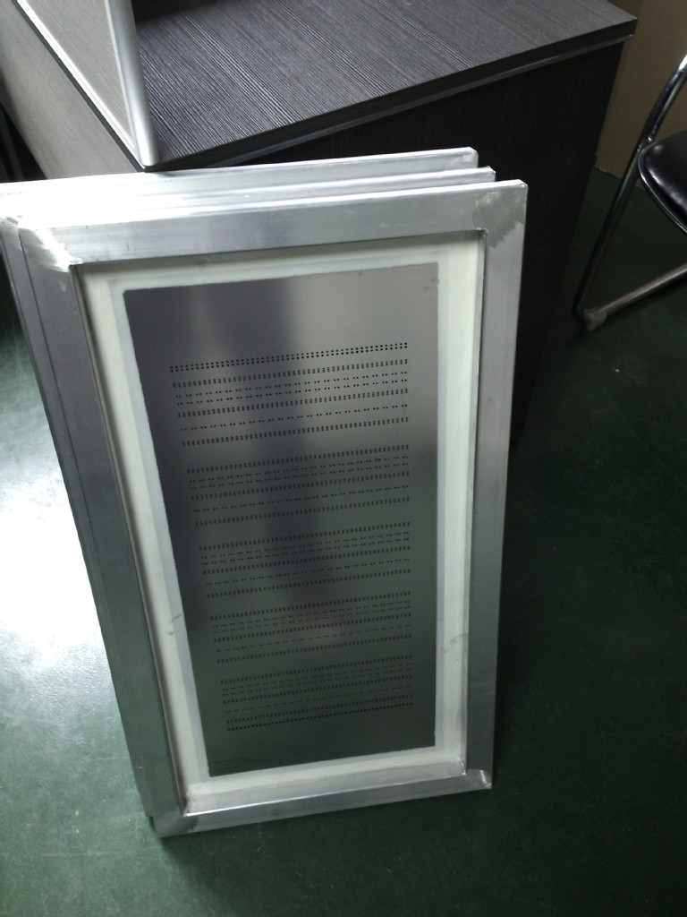
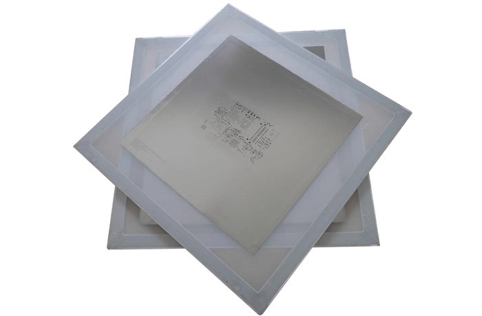
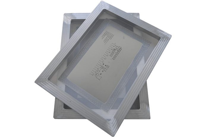
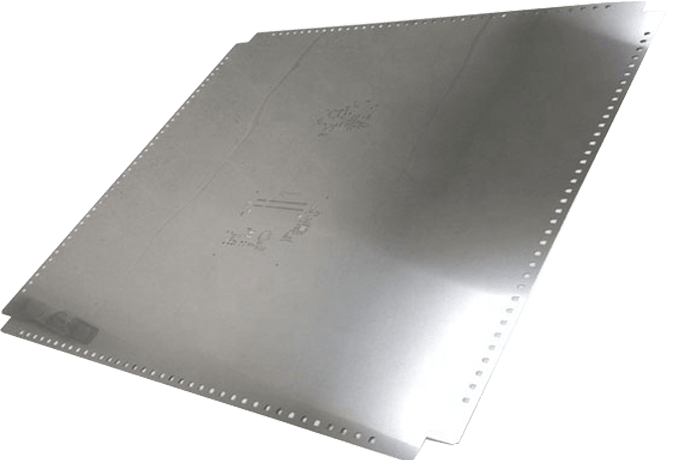
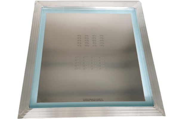
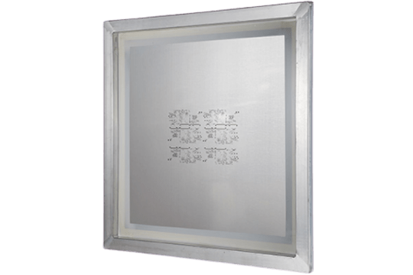
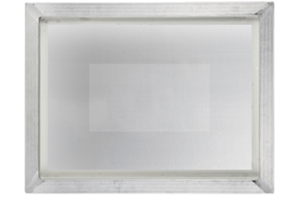
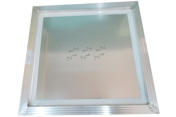
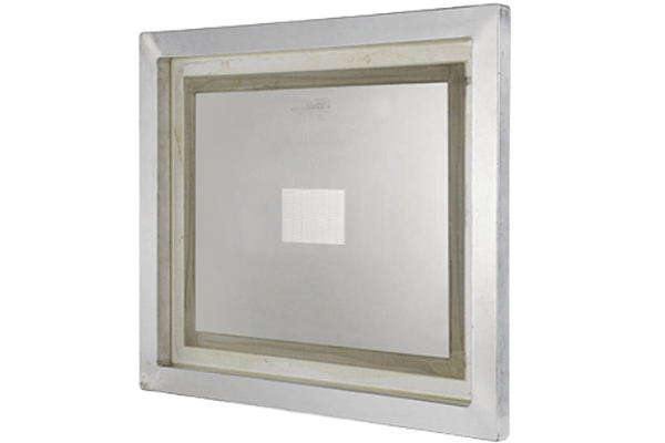
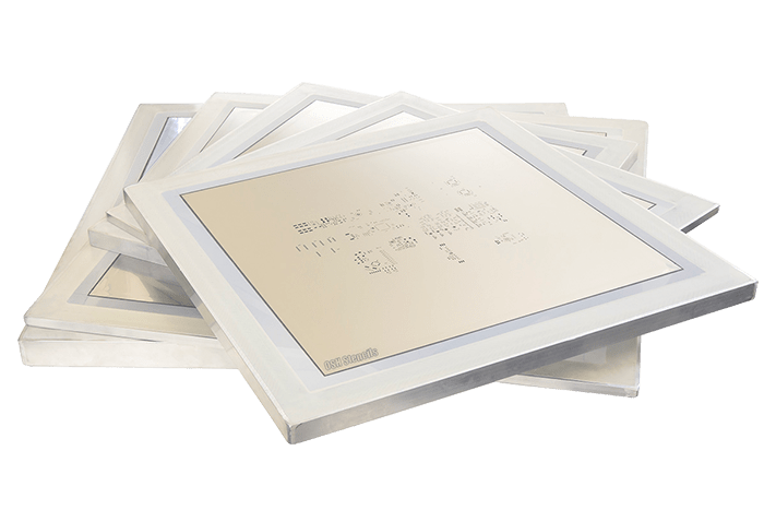
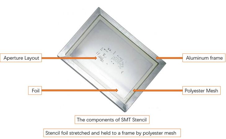
A framed PCB stencil will have a 0.5″ to 1.5″ thick metal frame around it, similar to a picture frame. Framed stencils are often used by contract manufacturers, assembly and board houses, and large scale production facilities and are commonly placed in a manual or automated stencil printing machine. Frameless stencils are a thin sheet of material cut with a small border around your design.none;”

All stencils are made with high-quality Polyimide and Stainless Steel. We use only the industry-leading Stainless Steel, explicitly designed for stencils. Stainless Steel: 0.0007″ Laser spot size, 0.001″ minimum aperture size. Polyimide Film: 0.003″ Laser spot size, 0.005″ minimum aperture size. Polyimide has a lower precision rate due to the way it is processed and its ability to withstand heat during the cutting process. Minor variances will occur when the material reacts to the laser. Paste release is excellent, but this material should be limited to a small number of uses and with components 0402 or bigger. The minimum aperture size for Polyimide is 0.005″ vs. 0.001″ for Stainless Steel. Polyimide also has a natural curl in the material caused by the way the film is manufactured; this is outside of our control. Stainless Steel provides the ultimate in precision and quality, with a 0.0007″ spot size, and exceptional paste release with a truly flat surface. If you want the absolute best reflow experience, there is no comparison, Stainless Steel is the superior material.
Stencil size is composed of two parts: internal size and overall size. Interior size is the size compatible with that of PCB ready to be assembled while the overall size refers to the format consistent with the printer parameter limit. As long as both dimensions are accurately designed, the stencil will be able to make full use of its functions. Internal size of stencil can be figured out conforming to the following rule: Width of Framed Stencil = width of PCB + 100mm while its Length = length of PCB + 100mm Width of Frameless stencil = width of PCB + 200mm while its Length = length of PCB + 200mm For example, if one circuit board size is 50*50mm, then the size of its framed stencil should be around 150*150mm, and the size of its frameless stencil should be around 250*250 mm. It’s easy to remember and operate, so it worked for manual solder paste printing in SMT assembly before the advent of the automatic printer. It can be said that different PCB sizes lead to generations of different internal dimensions of the stencil. When it comes to automatic solder paste printer, however, it’s relatively stable. The overall size of the stencil has to be determined by the parameter limit of the equipment, that is, printer because stencil has to work within the range of a printer with a frame. Different printers feature different parameter regulations. As far as JHYPCB is concerned, the stencil size compatible with our printer can be either 650mm*650mm or 736mm*736mm. PCB designers have to focus on the internal size of the stencil; they don’t need to care about its overall size since it is generally determined by the parameters of the printer in your contract assembler workshop.

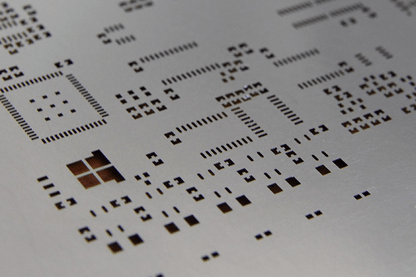
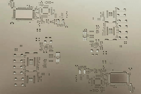
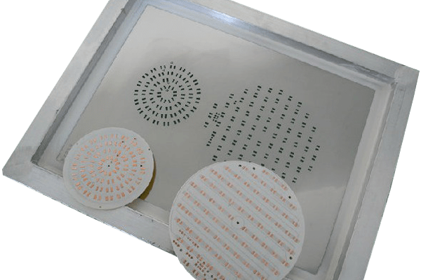
When the QFP pitch ≤ 0.5mm, the sheet thickness can be selected as either 0.13mm or 0.12mm; If the pitch> 0.5mm, then the steel thickness can be between 0.15mm – 0.20mm; If the BGA ball pitch > 1.0mm, then select a 0.15mm thickness. If the 0.5mm≤BGA ball pitch ≤1.0mm, then select a 0.13mm thickness.

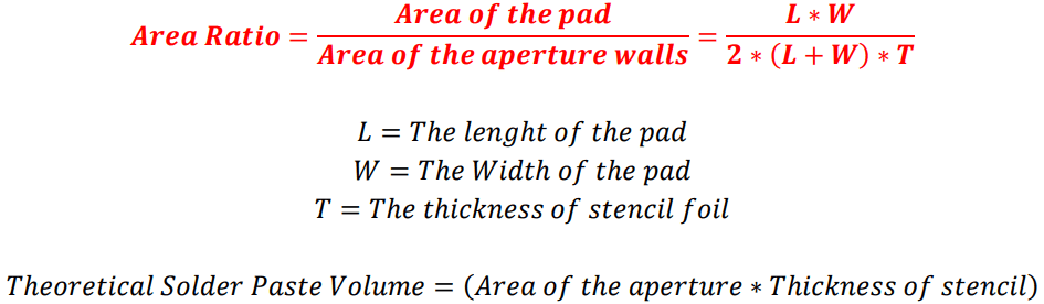
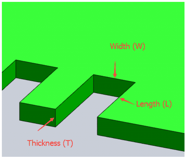
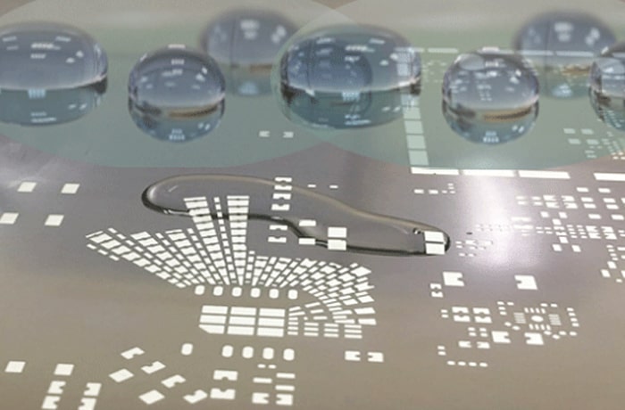
The stencil aperture is designed to match the land area on the PCB. It is recommended to use a pad to aperture aspect ratio of 90% to 100% with a recommended stencil thickness of 0.125mm.

SMT stencil wipes, also known as automatic wiping rolls, use natural wood pulp and polyester fiber as raw materials and are processed by a unique spunlace method.

SMT Stencil Wipes

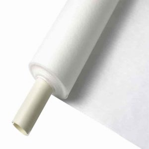
Features of SMT stencil wipes

SMT stencil wipes have the characteristics of durable, soft, dust-free, roll shape, strong tensile strength, efficient water and oil absorption, and anti-static.

SMT stencil wipes apply to SMT production lines, semiconductor assembly lines, optical products, PCB products, medical equipment, etc. It is advantageous for SMT factories to remove excess solder paste and red glue on the SMT stencil and circuit boards and keep circuit boards clean to reduce the scrap rate significantly and vastly improve production efficiency and product quality. To improve work efficiency, save expenses, and effectively control the dosage of SMT stencil wipes, the width and length of wipes can be selected according to the actual use.

SMT stencil wipes apply to all automatic solder paste printing models such as MPM, DEK, KME, Yamaha, Minami, JUKI, ekra, Panasert, Fuji, Sanyo, etc.

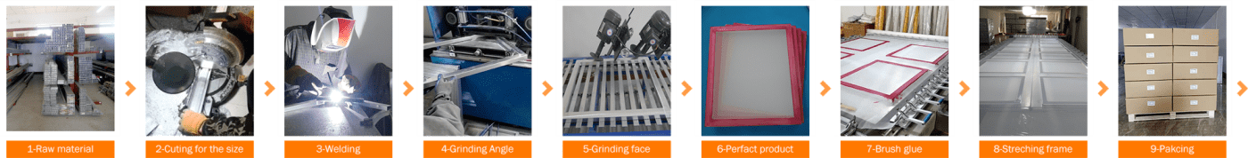
Information required for fabrication of SMT stencil:

  • Production requirements
  • SMT Stencil Use: Paste Solder Stencil or red Glue stencil
  • Polishing process: Polishing or electrolytic polishing
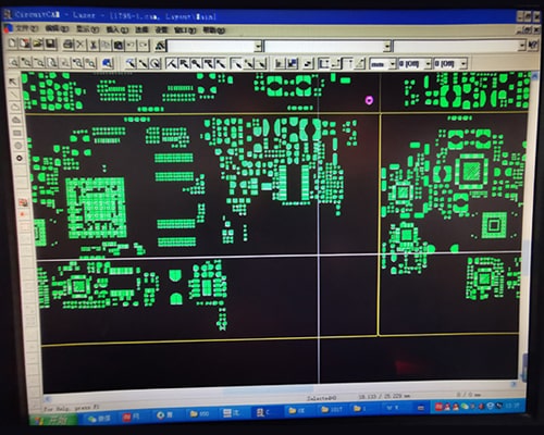
  • PCB file(GERBER、AUTOCAD、PCB、GBX.etc)
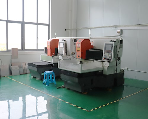
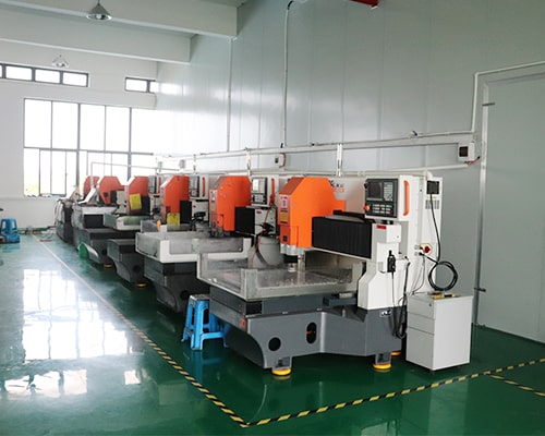
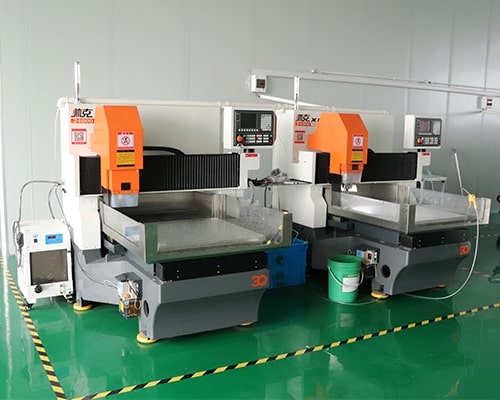
  • Fabrication Process:Laser-cut.etc
  • SMT Stencil Size
  • Frame or Frameless
  • SMT Stencil Thickness(The thickness of the steel sheet is determined by the smallest PITCH of the parts on the PCB)
  • Lead or Lead-free

The main factors affecting the quality of PCB stencils are:

  • Fabrication process
  • Materials
  • Opening design
  • Completeness and accuracy of production
  • Whether it is used properly
  • Cleaning
  • storage

Scroll to Top