
PCB Copper Thickness Capabilities
Learn about PCB copper thickness, also called copper weight, an important factor defining current capacity and impedance. JHYPCB specializes in heavy copper boards from 0.5-6oz to meet high power needs, offering superior heat dissipation and lower resistance.
Home » PCB Manufacturing Capabilities » PCB Copper Thickness Capabilities
What is PCB Copper Thickness?
PCB copper thickness, also referred to as PCB copper weight, is one of the most crucial factors in printed circuit board design. Copper thickness denotes the weight of copper per square foot area, defined in ounces (oz/ft2). The current carrying capacity of a PCB is entirely dependent on the thickness of the copper traces. Copper thickness is also considered when calculating trace impedance in high-speed and RF digital circuits. PCB copper weight requirements can vary based on the intended application and current carrying needs. At JHYPCB, we offer various copper thickness options to match clients’ specific PCB design requirements.
Key Points About PCB Copper Thickness:
- Copper thickness determines the current carrying capacity of a PCB
- Copper thickness must be factored when calculating trace impedance
- PCB copper requirements differ based on the application
- JHYPCB provides multiple thickness options to meet customer needs
Understanding 1oz Copper Thickness
In the PCB industry, copper thickness is commonly expressed in ounces (oz) – a unit of weight rather than distance. This stems from how copper foil was originally produced. When 1 ounce (28.35 grams) of copper is rolled flat to cover an area of 1 square foot (0.093 sq meters), the resulting foil thickness works out to 1.37 thousandths of an inch (mils). In metric units, 1 oz/ft2 copper equals 0.0348mm. So an “1 oz copper trace” implies a foil thickness equivalent to 1.37mils/0.0348mm. This convention allows thinner or thicker copper to be conveniently specified in oz/ft2 as well. A conversion chart is provided below for reference:
- 1⁄2 oz = 0.68 mils = 0.017 mm
- 1 oz = 1.37 mils = 0.035 mm
- 2 oz = 2.74 mils = 0.070 mm
- 3 oz = 4.11 mils = 0.105 mm
The ounce-based system stems from the early days of copper processing but lives on as a convenient way to denote foil thickness in PCB design and manufacturing.
Typical PCB Copper Weights
Inner Layers
- 1⁄2 oz (0.7 mils): We offer 0.5oz copper for inner layers, often preferred for specialized or non-standard boards requiring thinner copper.
- 1 oz (1.4 mils): Our standard copper thickness for inner layers, providing reliable conductivity at a moderate weight. Total finished thickness equals 2 oz with outer layers.
- 2 oz (2.8 mils): A common inner layer thickness when aiming for a total of 3 oz (1 oz outer layer plus 2 oz inner layer). This hits the sweet spot between higher conductivity and minimizing weight.
Outer Layers
- 1⁄2 oz (0.7 mils): Frequently used for external layers when inner copper thickness is specified at 1 oz. Combined total finished thickness equals the standard 2 oz.
- 1 oz (1.4 mils): Our standard outer layer copper thickness, offering proven reliability.
The above specifications allow Pick & Placing the optimal copper weight(s) tailored to your particular design needs and current carrying requirements.
| Track Width (inch) – The amount of current and temperature that a copper PCB can safely carry. | ||||||||||
|---|---|---|---|---|---|---|---|---|---|---|
| Cu weight (oz/ft2) | Thickness (inch) | 0.0625 | 0.1250 | 0.2500 | 0.5000 | 1.0000 | 2.0000 | 4.0000 | 8.0000 | 16.0000 |
| 1 | 0.0014 | 4.6 | 7.6 | 12.5 | 20.7 | 34.2 | 56.6 | 93.6 | 154.7 | 255.6 |
| 2 | 0.0028 | 7.6 | 12.5 | 20.7 | 34.2 | 56.6 | 93.6 | 154.7 | 255.6 | 422.5 |
| 4 | 0.0056 | 12.5 | 20.7 | 34.2 | 56.6 | 93.6 | 154.7 | 255.6 | 422.5 | 698.4 |
| 6 | 0.0084 | 16.8 | 27.8 | 46.0 | 76.0 | 125.5 | 207.5 | 343.0 | 566.9 | 937.1 |
| 8 | 0.0112 | 20.7 | 34.2 | 56.6 | 93.6 | 154.7 | 255.6 | 422.5 | 698.4 | 1154.4 |
| 10 | 0.0140 | 24.4 | 40.3 | 66.5 | 110.0 | 181.8 | 300.5 | 496.7 | 821.1 | 1357.1 |
| 12 | 0.0168 | 27.8 | 46.0 | 76.0 | 125.5 | 207.5 | 343.0 | 566.9 | 937.1 | 1548.9 |
| 14 | 0.0196 | 31.1 | 51.4 | 84.9 | 140.4 | 232.0 | 383.6 | 634.0 | 1047.9 | 1732.1 |
| 16 | 0.0224 | 34.2 | 56.6 | 93.6 | 154.7 | 255.6 | 422.5 | 698.4 | 1154.4 | 1908.1 |
| 18 | 0.0252 | 37.3 | 61.7 | 101.9 | 168.4 | 278.4 | 460.2 | 760.7 | 1257.3 | 2078.2 |
| 20 | 0.0280 | 40.3 | 66.5 | 110.0 | 181.8 | 300.5 | 496.7 | 821.1 | 1357.1 | 2243.2 |
| 24 | 0.0336 | 46.0 | 76.0 | 125.5 | 207.5 | 343.0 | 343.0 | 937.1 | 1548.9 | 2560.2 |
| 28 | 0.0392 | 51.4 | 84.9 | 140.4 | 232.0 | 383.6 | 634.0 | 1047.9 | 1732.1 | 2863.0 |
| 32 | 0.0448 | 56.6 | 93.6 | 154.7 | 255.6 | 422.5 | 698.4 | 1154.4 | 1908.1 | 3154.0 |
| 36 | 0.0504 | 61.7 | 101.9 | 168.4 | 278.4 | 460.2 | 760.7 | 1257.3 | 2078.2 | 3435.1 |
| 40 | 0.0560 | 66.5 | 110.0 | 181.8 | 300.5 | 496.7 | 821.1 | 1357.1 | 2243.2 | 3707.8 |
| 45 | 0.0630 | 72.5 | 119.8 | 198.0 | 327.3 | 541.0 | 894.3 | 1478.1 | 2443.2 | 4038.3 |
| 50 | 0.0700 | 78.2 | 129.3 | 213.7 | 353.3 | 584.0 | 965.2 | 1595.5 | 2637.1 | 4358.9 |
| 55 | 0.0770 | 83.8 | 138.6 | 229.0 | 378.6 | 625.7 | 1034.3 | 1709.6 | 2825.8 | 4670.8 |
| 60 | 0.0840 | 147.6 | 244.0 | 403.2 | 666.5 | 1101.7 | 1820.9 | 3009.8 | 4974.9 | |
| 70 | 0.0980 | 165.0 | 272.8 | 450.9 | 745.3 | 1231.9 | 2036.2 | 3365.7 | 5563.1 | |
| 80 | 0.1120 | 181.8 | 300.5 | 496.7 | 821.1 | 1357.1 | 2243.2 | 3707.8 | 6128.6 | |
| 90 | 0.1260 | 198.0 | 327.3 | 541.0 | 894.3 | 1478.1 | 2443.2 | 4038.3 | 6675.0 | |
| 100 | 0.1400 | 213.7 | 353.3 | 584.0 | 965.2 | 1595.5 | 2637.1 | 4358.9 | 7204.8 | |
| 120 | 0.1680 | 403.2 | 666.5 | 1101.7 | 1820.9 | 3009.8 | 4974.9 | 8223.0 | ||
| 140 | 0.1960 | 450.9 | 745.3 | 1231.9 | 2036.2 | 3365.7 | 5563.1 | 9195.3 | ||
| 160 | 0.2240 | 496.7 | 821.1 | 1357.1 | 2243.2 | 3707.8 | 6128.6 | 10130.0 | ||
| 180 | 0.2520 | 541.0 | 894.3 | 1478.1 | 2443.2 | 4038.3 | 6675.0 | 11033.1 | ||
| 200 | 0.2800 | 584.0 | 965.2 | 1595.5 | 2637.1 | 4358.9 | 7204.8 | 11908.9 | ||
Note: Approximate current for given track dimensions (20°C temp rise).
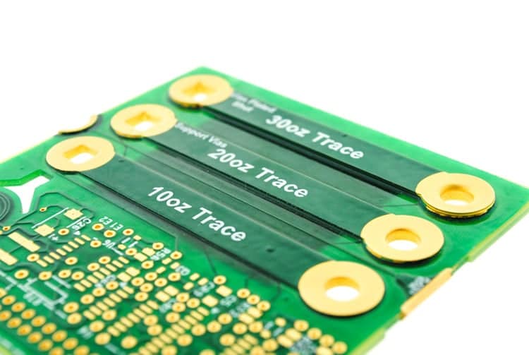
A heavy copper PCB is a PCB fabricated with thick copper foil layers. Like standard density PCBs, heavy copper boards contain conductive traces, plated through holes and pads. However, unlike standard boards, heavy copper PCBs utilize much thicker copper foil (typically 1-3 ounces per square foot), allowing them to carry higher current loads.
The thick copper on a heavy copper PCB enables:
- Increased current carrying capacity. The thicker copper can handle higher amperages and wattages.
- Superior heat dissipation. The extra copper provides more surface area to dissipate heat.
- Lower resistance. A thicker conductor leads to less resistive losses.
- Better power distribution. Heavy copper PCBs excel in power applications.
Heavy copper boards find application in high-power electronics where significant current must be delivered with low voltage drop across traces. Some common examples include:
- Power conversion circuitry
- Motor/servo control boards
- LED lighting
- Battery charging systems
- High-power computing hardware
At JHYPCB, we specialize in manufacturing complex and unique heavy copper PCBs tailored to your specific design requirements.
JHYPCB's PCB Copper Thickness Capabilities
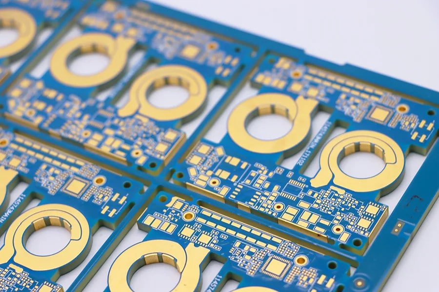
JHYPCB is a leading Chinese PCB manufacturer specializing in heavy copper PCB production and manufacturing services. We have extensive capabilities when it comes to PCB copper thickness for both inner and outer layers.
Inner Layer Copper Thickness
We can manufacture inner-layer PCBs with the following copper thickness options:
- 0.5 oz copper
- 1 oz copper
- 2 oz copper
- 3 oz copper
- 4 oz copper
- 5 oz copper
- 6 oz copper
Outer Layer Copper Thickness
For outer layers, we can provide PCBs with the following copper thicknesses:
- 1/3 oz copper
- 0.5 oz copper
- 1 oz copper
- 2 oz copper
- 3 oz copper
- 4 oz copper
- 5 oz copper
- 6 oz copper
- 10 oz copper
- 15 oz copper
With over a decade of experience manufacturing heavy copper PCBs, JHYPCB has the technical expertise to fabricate boards with demanding copper thickness requirements. We have an extensive production capability able to handle small prototypes to large volume orders.
Don’t hesitate to contact us to learn more about our PCB copper thickness capabilities or to request a quote for your next PCB project requiring heavy copper boards. We look forward to discussing how we can meet your specific requirements.
Useful Resources - Determining Your PCB Copper Needs
By a wide margin, most PCBs are fabricated with 1 oz copper on each layer. If your design files do not specify a target finished copper weight through a fabrication print or other instructions, we will assume 1 oz finished copper per layer as the default.
If your application requires higher operating voltages, lower resistivity, specific impedances, or other electrical performance metrics, a thicker copper weight may be necessary. There are several online trace width/thickness calculators that can assist in determining the appropriate dimensions and copper thickness to achieve your targets. We have provided links to a few commonly used free calculators below for reference – note that JHYPCB is unaffiliated with these tools or their authors.
We recommend considering the intended operating parameters and environmental conditions for your PCB early in the design phase. JHYPCB’s engineering team is ready to provide customized guidance and copper weight recommendations to ensure your board is optimized for the application requirements. Drawing on extensive experience, we can advise on best practices for copper thickness in everything from high frequency to high power designs. Please reach out for personal assistance tailoring the copper weights specifically for your project.