Home » Industries Served » PCBs for Communication Equipment
PCBs for Communication Equipment
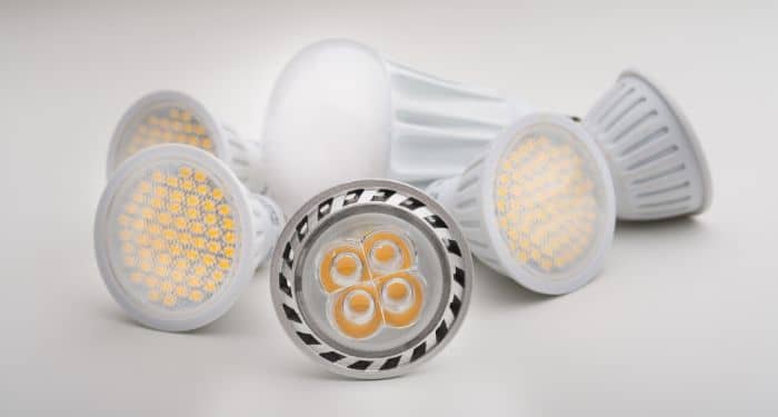
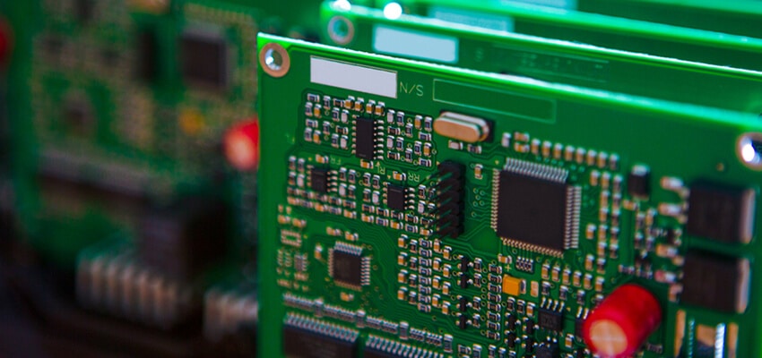
With the rapid development of information and communication technologies, electronic devices like smartphones, wireless routers, base stations and other communication equipment have become indispensable in daily life and work. The printed circuit boards in these devices serve as the foundation for assembly of components and integrated circuits, enabling the transmission of high-speed signals and data that make communication possible.
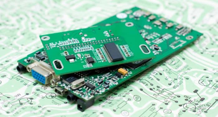
Communication device PCBs facilitate interconnections between active and passive components using conductive copper traces etched from copper-clad laminate boards. They provide mechanical support and the necessary electrical connections dictated by the intended functioning of the device. But most importantly, PCBs designed for communications applications must transmit signals accurately and reliably between components, without unacceptable loss or interference. This requires specialized materials and fabrication processes to serve the unique demands of high-frequency communication electronics.
At JHYPCB, we have rich expertise in manufacturing PCBs for all kinds of communication devices, from consumer electronics to telecom infrastructure. Leveraging over a decade of experience serving major brands globally, we fully understand the stringent requirements and can reliably produce communication PCBs for the most demanding applications. Whether prototyping bleeding-edge designs or volume production of complex boards, we have the capabilities to deliver.
Telecommunications Industry PCBs
Communication is the most important downstream application field of PCB. PCB has a wide range of applications in various aspects such as wireless network, transmission network, data communication and fixed network broadband, and it is usually added value such as backplane, high-frequency high-speed board, and multi-layer PCB board. Higher product. 5G is the next generation mobile communication network, and there will be a large amount of infrastructure construction demand by then, which is expected to greatly boost the demand for communication boards. Here are the most common applications of the telecommunication industry that make efficient use of PCBs:
- Wireless communication systems
- Mobile phone tower systems
- Telephonic switching systems
- PBX systems
- Industrial wireless communication technology
- Technology for commercial phones
- Video conferencing technologies
- Communication technology used in space
- Cell transmission and tower electronics
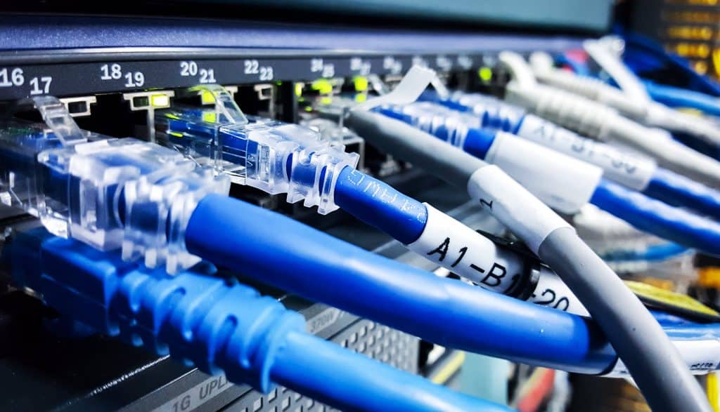
- High speed servers and routers
- Electronic data storage devices
- Mobile communication systems
- Satellite systems and communication devices
- Video collaboration systems
- Land wired communication systems
- Technology for commercial phones
- Digital and analog broadcasting systems
- Voice over Internet Protocol (VoIP)
- Signal boost systems (online)
- Security technology and information communication systems
PCB requirements in the communications field can be divided into sub-fields such as communications equipment and mobile terminals. Among them, communication equipment mainly refers to the communication infrastructure used for wired or wireless network transmission, including communication base stations, routers, switches, backbone network transmission equipment, microwave transmission equipment, fiber-to-the-home equipment, etc.
PCB Requirements
Communication devices require PCBs to provide robust and reliable connectivity solutions for complex high speed components. Signal integrity needs to be maintained as signals travel between transceivers, antennas, power amplifiers and more. These requirements generally include:
- High-Frequency Performance
Many communication device signals operate at high frequencies in the microwave band. For example, smartphones incorporate multiband antennas that support 4G and 5G frequency bands – 700 MHz to 5 GHz for the latest generation. This requires PCB materials and construction to enable proper signal transmission without degradation through dielectric power loss or leaky RF conduction paths. We carefully select substrates and lamination materials tailored for high frequency operation based on dielectric constant, loss tangent, thermal conductivity, TCE and other parameters. - High Speed Signal Handling
In addition to frequency, data rate throughput capacity is equally important. Cutting-edge phones with multi-Gbps Wi-Fi 6 speeds, high bandwidth wireless interfaces need PCBs with fine line traces and spaces (4-6 mil line/space is common for data lines). Short signal paths routed close together require low loss, tight impedance tolerance laminates as well as careful stackups for characteristic impedance control. And a robust power distribution network is key for clean power delivery to signal ICs and FPGAs operating at high clock rates. We design layer counts, trace dimensions, dielectrics and laminate materials specifically to maintain signal integrity in high speed signal paths. - EMI and Crosstalk Prevention
With complex components in close proximity and interacting at high frequencies, communication PCBs must prevent unwanted coupling between traces. Short signal return paths, reference planes and proper component placement facilitate field confinement. Our engineers utilize careful stackup symmetry, selective isolation/shielding around sensitive components, ground stitching vias alongside traces, and special treatments to eliminate EMI emission and minimize crosstalk in dense layouts with high speed traces throughout multilayer boards.
PCB Materials
Engineering the optimal PCB solution for communication products necessitates careful material selection for the substrate laminates, prepregs, conductive layers, coatings, and finishes. We utilize an array of specialized materials tailored for the electrical, mechanical, and environmental performance criteria required by these demanding applications.
- FR-4
The workhorse of PCB substrates, FR-4 glass reinforced epoxy, offers a baseline of electrical insulation performance, mechanical rigidity, and environmental integrity at economical pricing. We use high-quality FR-4 cores and prepregs from leading Asian suppliers, and have contractual partnerships to ensure a stable supply of consistent materials, certified to meet both IPC and our own stringent QC requirements. - High Frequency Laminates
Communication systems operating past 1GHz require low loss circuit board dielectrics. We offer a range of high frequency/low loss laminates including Rogers RO4000, RO3000 and RT/duroid series, Isola, Taconic TLY and TFLY families and others for microwave applications. Careful selection of dielectric constant and loss tangent allows impedance matching for optimal signal integrity at intended operating frequencies and data rates. Materials are tested through design/fab/test correlation vehicles to validate modeled electrical performance. - PTFE Based Composites
For extreme environmental tolerance and stability at microwave frequencies, ceramic-filled PTFE substrates like Rogers’ RT/duroid 6202PR demonstrate outstanding lifetime performance under severe thermal cycling and corrosive conditions like avionics applications require. The dimensionally stable PTFE matrix with low Dk ceramic filler enables fabricating 2.5D glass microvia interconnects ideal for high frequency front end modules.
Our technology portfolio includes a diverse PCB solutions toolkit ready to serve the varied needs and applications spanning communication systems design landscapes. We offer expertise catering to essential requirements from thermal management to signal integrity to lightweighting across product generations. Various PCB platforms seen in our customer programs:
- Rigid PCB Boards
The majority of communication circuit designs leverage cost-effective rigid laminates like FR4 in multilayer constructions for routing density and performance – we build complex boards up to 36 layers and beyond. Rigid-flex PCBs integrate flexible circuits extending interfaces. - HDI PCB Boards
Embedding precision thin dielectrics down to 2-4mil lines/spaces using laser microvias enables the finer pitch, higher IO density critical in wireless front end modules, power amplifiers and more as devices evolve smaller. We implement stacked microvia HDI technologies in high layer count configurations suitable for integration functionality. - RF/Microwave Laminates
High frequency antenna arrays, radar and sensitive receive path electronics often demand specialized low loss laminates. We select from Rogers, Taconic and other premium RF/microwave materials based on tolerance requirements and application parameters like thermal conductivity.
PCB Technology and Testing
Leveraging advanced PCB fabrication processes and testing methods ensures the signal and power integrity necessary for high reliability communication products. We utilize cutting-edge manufacturing technologies aligned with rigorous testing capabilities tailored for these demanding applications:
- Fine Line PCB Technology
The increasing digital complexity and data rates of communication electronics requires smaller, denser PCB traces and spaces. Our line/space capabilities down to 3/3mil with registration accuracy of 2.5um facilitates complex radio designs. We combine laser direct imaging pattern generators and high precision mechanical drilling equipment to produce incredibly intricate circuit patterns throughout multilayer boards without compensation. - Controlled Impedance PCBs
Maintaining tight impedance tolerance across traces and achieving desired differential impedance for differential pair signals is critical for RF and high speed digital PCBs. Both fabrication process consistency and verification testing capacity are essential to deliver controlled impedance PCBs. We implement automated lamination pressure, temperature and time monitoring along with microsection cross-sections to dial in and match impedance targets. - Signal Integrity Testing
To characterize signal loss and reflection behaviors in fabricated designs, we utilize high speed testers including Vector Network Analyzers to analyze S-parameters, time domain reflectometry and other metrics to fine tune processes for optimal SI performance. Test coupons with device geometries, lines, vias, materials, layer stacks representative of customer boards provide correlation data ensuring first time success. We work closely with clients through DFM reviews to develop fabrication test vehicles for their unique technology requirements.
Quality and Reliability
Delivering the highest reliability PCB solutions for mission-critical communication systems demands strict process and quality management upholding industry standards. As an ISO 9001 certified manufacturer, we’ve implemented robust infrastructure spanning materials qualification to volume fabrication monitoring:
- IPC Standards
We benchmark quality against IPC J-STD-001, IPC-A-600 and other widely adopted PCB quality specifications. Audits of our facilities verify standard classes conformance through acceptance testing of fabricated boards as well as process reviews targeting continual improvement per IPC guidelines. IPC certifications validate disciplined, optimized fabrication workflows. - Advanced Quality Planning
Reliability risks are systematically identified during NPI through process controls selection, PFMEA/DRBFM and test vehicle measurements establishing performance baselines. We tailor process qualification, verification testing and QA sampling plans per customer requirements and design risk assessments. Each producible design has associated quality plan generating 1st pass yields. - Traceability
Raw materials receipt to finished boards shipped are tracked by ERP software tools with batch/lot traceability. Barcode work orders follow boards through process documenting each fabrication, inspection and test operation in our secured database. Complete traceability with records retention delivers the transparency customers expect from their trusted PCB producers.
Our Capabilities
With over a decade of experience serving communication leaders, we leverage extensive expertise transforming designs into high performance, reliable PCB solutions ready for the most challenging next-gen programs. We continue targeting innovation improving technical capabilities and service quality for this dynamic industry.
- Technology Leadership
Early investments in advanced equipment like laser drill/direct imaging enable leading-edge process capabilities. We collaborate closely with supply chain partners including key material vendors driving materials science breakthroughs accelerating next generation performance. Our engineers engage with industry consortiums and associations furthering technical knowledge. - Manufacturing Excellence
Efficient, flexible production workflows allow responding rapidly while controlling costs, via optimized factory layouts, strategic supplier integration and continuous improvement drives. ISO certified quality management systems assure consistency through rigorous product and process monitoring procedures. We pass audits from top global OEM firms regularly while achieving 90%+ on-time delivery rates. - problem-Solving Culture
Our veteran engineering team loves solving tough PCB challenges together with clients through collaborative engagements. Whether tackling signal integrity issues during prototyping or overcoming exotic material sourcing for cutting edge designs, we get creative finding solutions. Years assisting clients turning concepts into fielded systems provides application insights adding value.
Conclusion
Continued exponential growth in mobile data and connectivity speed fueled by 5G rollout is driving relentless innovation in communication hardware. As a premier PCB solutions provider catering to this dynamic industry for over a decade, JHYPCB stands ready to partner with forward-thinking brands in realizing next generation designs.
Leveraging substantial expertise serving top telecom infrastructure, networking and consumer electronics leaders, we offer the technical capabilities required to fabricate complex, high frequency PCBs. Whether an emerging startup building revolutionary wireless systems or an established industry player enhancing networks, we empower innovation from prototype through volume production.
With customer focused project management combining collaborative problem solving attitude and veteran engineering know-how, JHYPCB delivers high quality, reliable PCB solutions ready for the most demanding communication programs. We aim to earn business through consistent on-time performance, transparent communication and ultimately enabling customer success.
Contact our application engineers to discuss your communication device PCB requirements and discover how we can deliver a winning partnership.
JHYPCB - Leading High-Quality, Quick-Turn PCB Manufacturing
At JHYPCB, we are a premier PCB manufacturer providing one-stop PCB fabrication and assembly services to meet the diverse needs across multiple industries. With years of experience and cutting-edge capabilities, we deliver high-quality, quick-turn PCB solutions tailored to each application’s unique requirements.
Our Core Expertise:
- High-reliability PCBs for demanding applications
- Wide range of PCB technologies: HDI, rigid-flex, RF/microwave, thermal boards, and more
- Advanced manufacturing processes: high-density interconnect, buried/blind vias and more
- Fast prototype to production cycle times
- Strong engineering support from quote to delivery
Whether you need prototypes for new product development or high-volume PCB production, JHYPCB is your trusted partner. Explore our PCB capabilities for your industry below.