
Low-cost Double-sided PCB Board Prototype Production service
Double Sided PCB, also known as Double Layer PCB, is a printed circuit board with conductive copper layers on both sides. JHY is a reliable PCB manufacturer, providing high-quality single-sided PCB, double-sided PCB, and up to 64 layers of multi-layer PCB prototype and mass production service.
Home » PCB Manufacturing » Double-Sided PCB
At JHYPCB, we are a leading PCB manufacturer in China specializing in high-quality double-sided PCBs. As an innovative company, we leverage the latest technologies and techniques to produce double-sided printed circuit boards that meet various design needs.
Double-sided PCBs provide advantages over single-sided boards for many applications due to their increased component density, flexible routing options, improved signal integrity, and overall optimized layout.
With years of experience manufacturing premium double-sided PCBs, JHYPCB is committed to delivering boards that enable your products’ best performance, quality, and reliability. Whether you require complex routing for multilayer circuits or maximum density for compact designs, we can fulfill your double-sided PCB requirements.
Double Sided PCB Definition
What is Double Sided PCB?
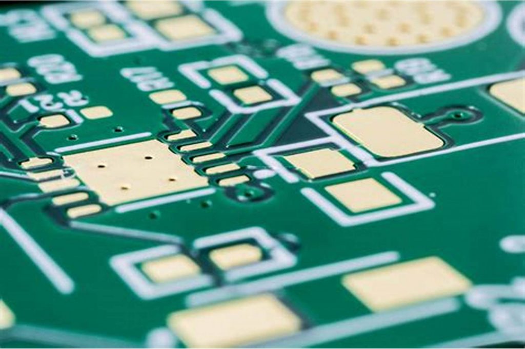
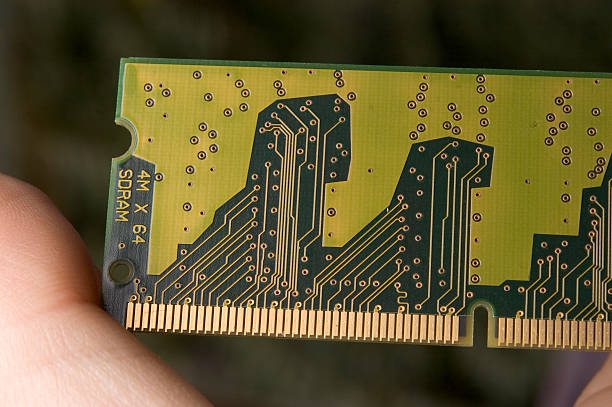
A double-sided PCB, also known as a double-layer PCB, 2 layer PCB, has two conductive layers: one at the top surface and one at the bottom of the PCB. It means the circuit and components can be on two sides.
There are two conductive layers in the double-sided PCBs, so they are used for tasks where single-layer PCBs cannot work. The back of the PCB board is also utilized to implement complex designs and get the most out of the space. Due to two conductive layers, the PCB can have more components in a small area, while a similar single-layer PCB can have half of the components.
These PCBs are more advantageous and are preferred for various applications. Double-sided is mainly used and preferred among all types of PCBs (single-layer, double-layer, and multilayer).
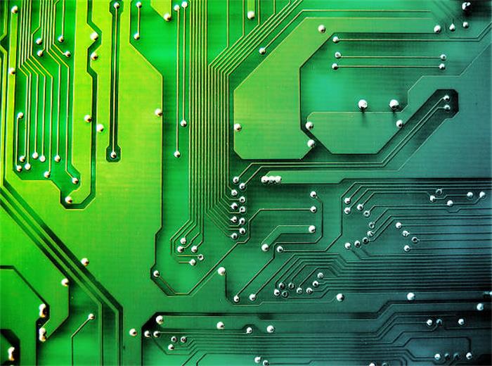
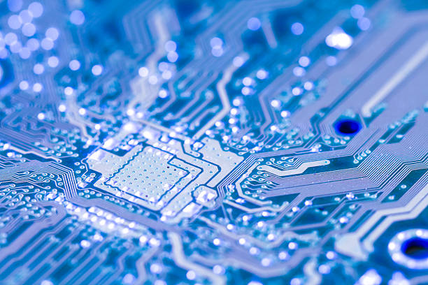
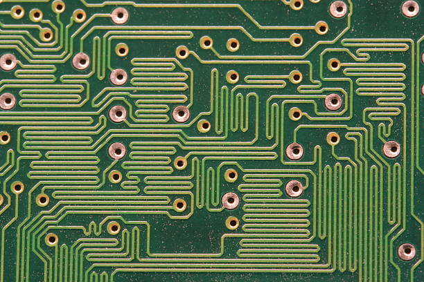
double sided circuit board
Types of double-sided PCB
Double-sided PCBs can be classified into different types. The types are,
- Double-sided Rigid PCB
- Double-sided Rigid-Flex PCB
- Double-sided Flexible PCB
- Double-sided Metal Core PCB
- Double-sided High TG PCB
- Double-sided High-Frequency PCB
- Double-sided Heavy Copper PCB
- Double-sided Impedance Control PCB
Everything You Want To Know About Double Sided PCB
Double Sided PCB Stack up
Stack-up in Double Sided PCB - Double sided PCB Design
The stack-up of a double-sided PCB is quite simple. You can assume it as two single-layer PCBs joined together.
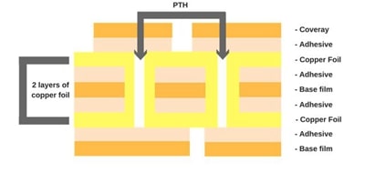
The top layer of a double-sided PCB is a conductive layer. After that, there is a dielectric layer in the center, which is the base material of the PCB. At the bottom, there is another conductive layer. Simply put, the dielectric/base layer is sandwiched between two conductive layers.
The conductive layer is made of copper, as it has excellent electrical conductivity and is also cost-effective. Gold or Silver can also be used to make a conductive layer or for its plating.
The base/dielectric layer could be made of various materials. It can be FR-4, Polyimide, PTFE, metal (aluminum, copper, or iron), or any other suitable substrate. If the base material is non-conductive, it behaves as an insulator between the two conductive layers. But if the base layer is metal, then a dielectric layer is also used to create insulation between the layers as it is necessary to prevent short circuits between the layers.
Other than the base and conductive layers, there are layers of surface finish, solder mask, and silkscreen. These layers are common in all types of PCBs as they provide extra benefits. The surface finish is for the protection of the copper layer, and it prevents oxidation and corrosion. It increases the life of the conductive layer. The solder mask also prevents the formation of solder bridges and unwanted connections. The silkscreen is used to label the components on the PCB board.
Related Reading: Standard PCB Thickness—All You Need To Know
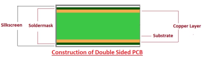
Construction of double-sided PCB
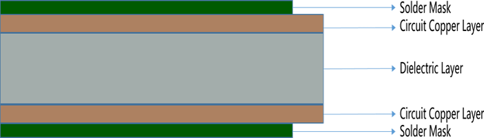
Double Sided PCB Layers
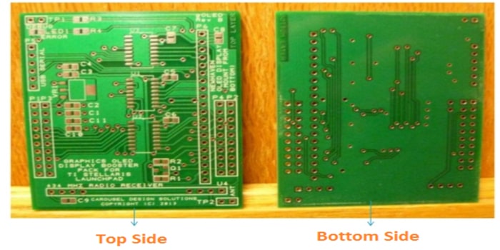
Double Sided PCB-Top Side and Button Side
Double-sided Flexible PCB Circuit Board
Double-sided Flexible PCB Stack-up
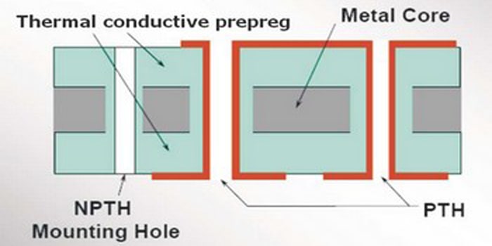
Structure of Double Sided MCPCB
Double Layer PCB Prototype Manufacturer
Double-Sided PCB Benefits
Advantages of Double Sided PCB
Double-sided PCBs provide several advantages over single-sided boards, making them an attractive choice for many electronics designs. Some of the key benefits include:
- Increased Component Density
One of the biggest advantages of a double-sided PCB is the ability to place components on both sides of the board, doubling the usable surface area. This allows for fitting more electronic components and circuitry into a compact space. For products where small size and miniaturization are critical, like mobile devices and wearables, maximizing component density is essential. The two-sided structure of a double-sided PCB enables layout optimization for density and small product footprints. - More Routing Options
With traces and vias on both layers of a double-sided PCB, designers have more flexibility for connecting components. Critical signals or high-speed traces can be routed on one side, while less critical traces occupy the other. This facilitates routing for complex and high-density designs. The top and bottom layers can also be assigned specific functions like power distribution or ground planes. Overall, the two circuit layers offer improved routing with less congestion. - Better Signal Integrity
Signal integrity refers to maintaining the quality and strength of signals as they propagate through a PCB. Running a continuous ground plane on the bottom layer of a double-sided board provides superior reference grounding for signals on the top layer. This provides better isolation from noise interference and ensures signals maintain integrity across the board. A solid ground plane is crucial for designs operating at high frequencies. - Increased Layout Optimization
A double-sided PCB layout can be highly optimized with the ability to place components and route traces on both sides. Components and routing can be arranged to minimize wire lengths, reduce crosstalk between traces, and meet emission requirements. Dense sections of the board can be intelligently divided between sides. Double-sided construction enables optimization not possible with single-sided boards. - Space-saving
The most important benefit of double-sided PCB is space-saving. It can save a lot of space as the components can be on both sides. Thus, it is half the size of a single-layer board. Due to high component density, more components are on the board, and every area is utilized. The final board is compact, which is why it can save space. Due to this advantage, designers try to use double-sided PCBs in their projects as they are less complex than multilayer PCBs and more compact than single-layer ones. These are mostly preferred where the size of the final product matters. - Cost-effective
A double-sided PCB is the best option to save money. If the circuit can be implemented on a double-sided PCB, then there is no need to spend a magnificent amount on multilayer PCBs. It provides a compact board at a lower price.
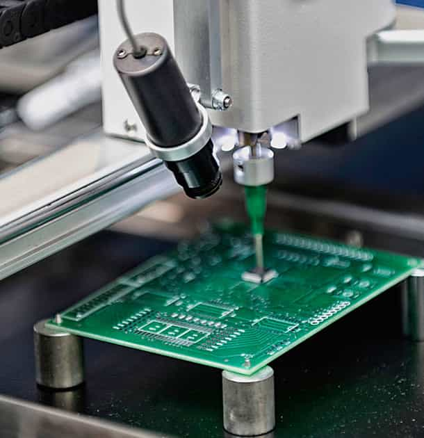
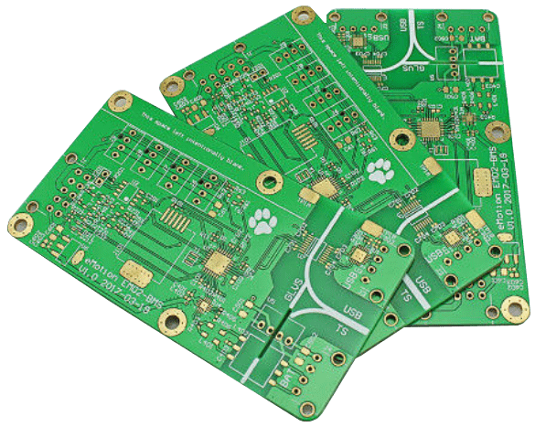
Double Sided PCB Board Prototype
Double Sided PCB Prototype Fabrication
As we all know, the double-sided circuit board is a very important PCB in the printed circuit board. The market has double-sided metal-based PCB, Hi-Tg heavy copper circuit board, double-sided flexible circuit board, and double-sided high-frequency circuit board.
The most common surface treatment used in manufacturing double-sided PCB board prototypes is OSP, immersion gold, lead-free tin spraying, etc.
The double-sided PCB with a lead-free tin spraying process has the advantages of beautiful appearance, white pads, easy-to-tin pads, ease-to-solder, and low price.
Double Sided PCB Fabrication Capability
JHY is a well-known double-sided PCB manufacturer in China specializing in building your double-sided PCB prototype and mass production with quick turns.
- Materials: FR4, Copper Core, Aluminum, Rogers…
- PCB Size: Max. 680mm*1200mm
- PCB Thickness: Custom
- Surface Finishes: OSP, Immersion Silver/Gold/Tin, Plated Gold, Flash Gold,…
- Solder Mask: Green, Red, White, Black, Blue, Yellow,.etc.
- And we can offer: double-sided FR4 PCB, double-sided copper-clad PCB, double-sided flexible PCB, double-sided rigid-flex PCB, and double-sided Rogers PCB fabrication service.
Double-Sided PCB Applications
Double-sided PCBs are widely used as they are cost-effective and can deal with complex circuitry. These PCBs are used in consumer electronics. You will find such PCBs in appliances used at your home, including juicer machines and LED lighting.
These PCBs are also used for advanced power applications, such as converters, inverters, UPS, and power supplies. The usage of double-sided PCBs has increased after the increase in the demand for renewable energy.
Industrial and commercial ventilation and cooling systems are also equipped with these PCBs. They are used in HVLS fans, evaporative coolers, and HVAC systems.
Industrial instruments and machines also have double-sided PCBs for controlling and performing the job.
You will also find these PCBs in printers, mobile phones, hard drives, remote controllers, sound systems, and other commonly used appliances and devices.
In simple words, double-sided PCBs are used in almost every sector, and if they can perform the desired task, it is better to use them.
- Industrial controls
- Power supplies
- Converters
- Control relays
- Instrumentation
- Regulators
- UPS systems
- Power conversion
- HVAC
- LED lighting
- Hard drives
- Printers
- Phone systems
- Power monitoring
- Automotive dashboards
- Line reactors
- Test equipment
- Amplifiers
- Traffic systems
- Vending machines
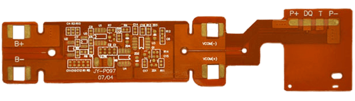
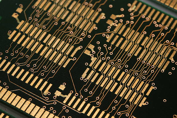
Doule-Sided PTH PCB
Key Differences: Single-Sided vs. Double-Sided PCBs
One of the first decisions when designing a PCB is whether to use a single-sided or double-sided board. While both have their applications, double-sided PCBs provide advantages that may be worth the additional cost for many designs.
Below is a comparison of key differences between single-sided and double-sided PCB boards:
| Category | Single-Sided PCB | Double-Sided PCB |
|---|---|---|
| Layer Count | One conductive layer | Two conductive layers |
| Component Placement | On one side only | Both sides allowed |
| Routing | Limited to one side | More flexible, both sides usable |
| Density | Lower component & routing density | Higher component & routing density |
| Ground Plane | No continuous ground plane | Can have ground plane on one side |
| Signal Integrity | Poorer, more susceptible to noise | Better, ground plane shields noise |
| Size | Larger | More compact |
| Applications | Simple circuits | High-density or high-frequency |
| Cost | Lower | Higher |
In summary, double-sided boards allow higher-density routing and better signal integrity for space-constrained designs but have higher costs. The optimal choice depends on the specific project requirements.
How To Make Double-sided PCB?
Double sided PCB Manufacturing Process
The PCB manufacturing process is very precise, difficult and complicated.
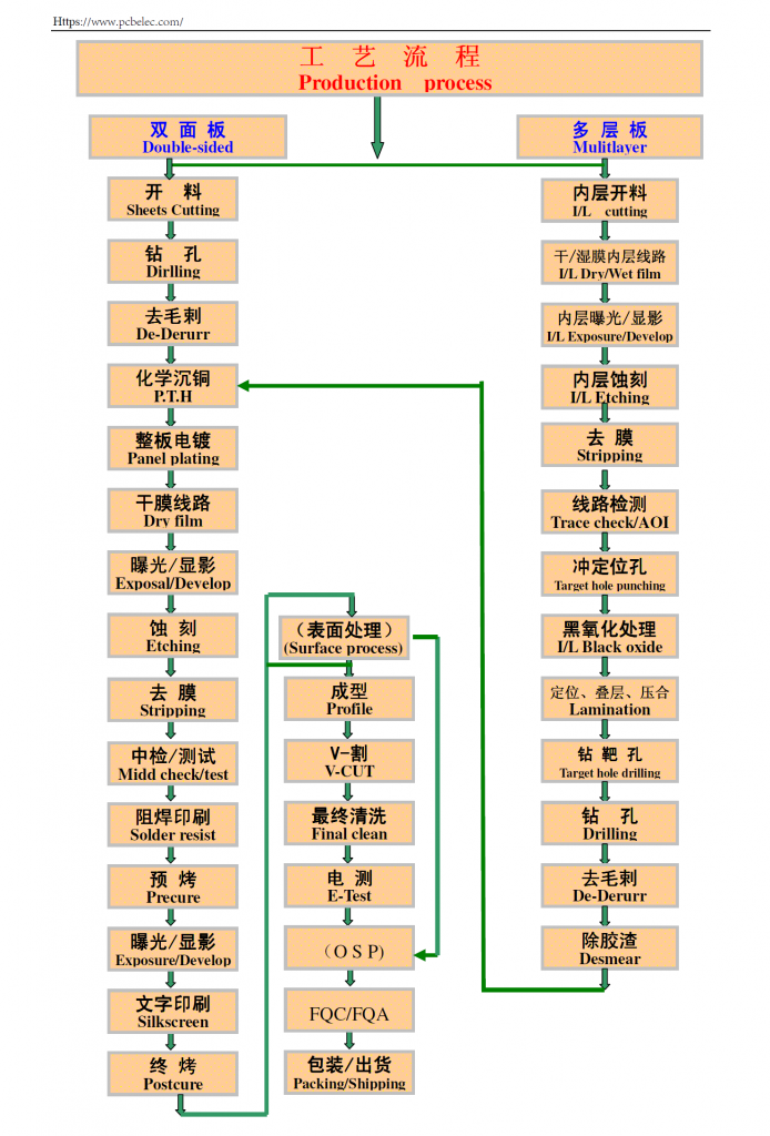
The rigorous manufacturing process ensures the quality and performance of electronic finished products. Although the circuit board can be divided into single-sided PCB, double-sided PCB, and multilayer PCB according to the number of layers of the conductor pattern, the manufacturing process used is only different after the first layer is produced. Please refer to the double-sided PCB and multilayer PCB manufacturing flow chart on the right for more information.
Double-sided PCB Manufacturing Process:DFM –> Sheeting Cutting –> Drilling –> De-Derurr –> P.T.H –> Panel Plating –> Dry Film –> Exposal / Develop –> Etching –> Stripping –> Midd Check/Test –> Solder Resist –> Precure –> Exposure / Develop –> Silkscreen –> Postcure –> Surface Process –> Profile –> V-cut –> Final Clean –> E-Test –> FQC / FQA –> Packing / Shipping.
Learn more about the double-sided PCB manufacturing process step-by-step guide.
The Double-Sided PCB and Multilayer PCB manufacturing Process Flowchart
The Double-sided PCB Soldering Process
How to make Double-sided PCB
Double Sided PCB Manufacturing- Etching
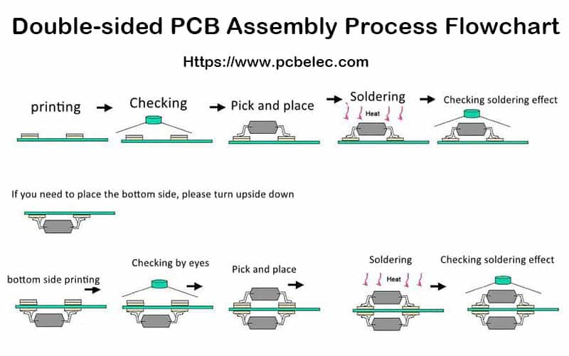
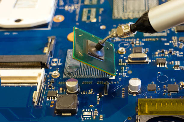
Double-Sided PCB Assembly
Double Sided PCB Assembly Process
SMT, the trendy surface mount technology in PCB assembly at present, is a technology for mounting and soldering surface mount components on a printed circuit board.
Double-sided PCB Assembly Process Step by Step:
Step 1: Solder Paste Printing
Step 2: Checking
Step 3: Pick and Place
Step 4: Sldering
Step 5: Checking Soldering Effect
If you need to place the bottom side, please turn upside down.
Step 6: bottom side printing
Step 7: Checking by eyes
Step 8: pick and place
Step 9: Soldering
Step 10: Checking Soldering Effect
Get Optimal Quality 2 Layer PCB prototype at JHYPCB
JHYPCB is a leading PCB manufacturer and assembler. We have a large facility with 500+ experienced employees. We can handle small to large volume orders, and there is no restriction on the minimum order quantity. You will get solutions to all your PCB problems and queries under one roof. Our facility is equipped with the latest technology, and we have experts that can deal with complex PCBs and assemblies. We are ISO, RoHS, and UL certified.
We can provide high-quality double-sided PCBs that can deliver optimal results. We can offer small to large volume PCBs at a low cost. You can take our services for prototypes and turnkey assembly. Our services are also perfect for startups and new projects as we can even deliver only one PCB or PCBA. For more information and details, feel free to contact us.
Recommended PCB Manufacturing Services
Related Posts
- Custom Circuit Board Printing
- Custom PCB Manufacturer In China
- Best PCB Manufacturer In China
- How To Search for a Reliable PCB Manufacturer
- PCB and PCBA Manufacturing Files
- Find Out Now, What Should You Do For Fast PCB Classification?
- What is a Multilayer PCB, and What Are the Advantages?
- Single-layer PCB vs. Double-sided PCB: How to Choose?
- How to Store PCB and PCBA?
- The Benefits Of Using Double Sided PCBs