
4-LAYER PCB TUTORIAL
DEFINITION, STACK UP, PROTOTYPE, AND MANUFACTURING COST
Home » PCB Manufacturing » Multilayer PCB » 4 Layer PCB
4-layer PCB is the most basic type of multilayer PCB, and it is a multilayer printed circuit board with the fewest circuit layers. 4-layer PCB is much more advanced than single layer or double layer PCB.
JHYPCB
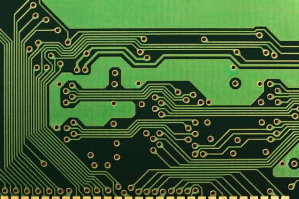
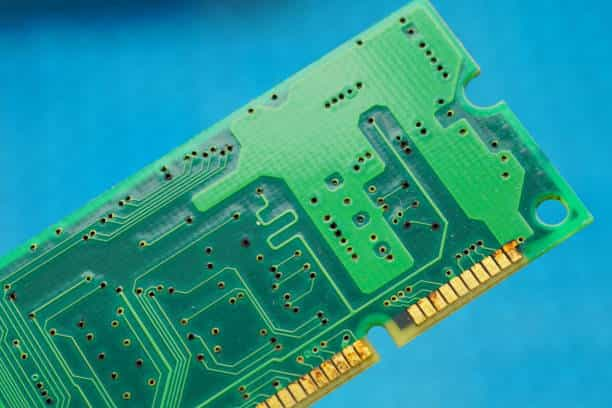
4 Layer PCB Prototype Manufacturing

As the demand for high-performance and miniaturized electronic products increases, the need for high-density and small-size PCBs has also expanded. As a result, the circuit board has become smaller than before, there are various designs to choose from, and they can be customized according to specific requirements. Therefore, various multilayer circuit boards have been developed, including 4-layer PCBs.
4-layer PCB is a standard multi-layer PCB that has many uses. Are you interested in learning more about them, especially their laminated design and types? What are their advantages, and how do they compare to double-layer PCBs? How to make a 4-layer PCB? This article will take you through all of this.
4-layer PCB Definition
What Is 4-Layer PCB?
PCBs can be made in multiple layers, according to your requirement. A multilayer printed circuit board contains three or more conductive layers, with the inner layer used to conduct signals or power. We can perform not every task with a two-layer PCB; therefore, there is a need for a 4-layer PCB.
A 4-layer PCB means that it has four layers. These four layers include two inner layers, one top layer and one bottom layer. Among these four layers, two are signal layers, one is VCC, and the remaining is GND.
Learn more about what are the classifications of PCBs?
Usually, inner layers are used as power and GND, and outer layers (top and bottom) are used for signal routing and component placement. The reason behind using inner layers as power and GND planes because it tends to reduce EMI emissions, and it also improves the quality of the signal. In a 4-layer PCB, it is simpler and easier to connect the components than routing power and GND planes along with traces. However, with us, you don’t need to worry about that. We provide every type of 4-layer PCB and prototype services at JHYPCB.
Multilayer Printed Circuit Board
What is a multilayer PCB?
The definition of multilayer PCB is a printed circuit board that is made with three or more conductive copper foil layers. These appear as several layers of double-sided PCBs, laminated and glued together with layers of heat-protective insulation between them. The entire construction is arranged so that two layers are placed on the surface sides of the circuit board to connect to the environment. All electrical connections between the layers are achieved with vias, such as plated through holes, blinds, and buried vias. Application of this method then leads to the generation of highly complex and high-end PCBs of varying sizes.
JHY is a reliable multilayer PCB manufacturer in China and one of the cheapest multilayer PCB manufacturers. In terms of high-end multilayer PCB manufacturing, we are equipped with the most advanced PCB manufacturing equipment to meet the most complex multilayer PCB manufacturing services.
Relying on our advanced PCB manufacturing capabilities, JHY provides all types of 4 layer PCB manufacturing services, such as 4 layer rigid PCB, 4 layer flexible PCB, 4 layer rigid-flex PCB, 4 layer aluminum PCB, 4 layer high Tg PCB, 1+ 2+1 HDI PCB, etc.
Lean more about What Are the Multilayer PCB Applications?
4 Layer PCB Stack up
Standard 4-Layer PCB Design Guide
There are three ways you can stack up a 4-layer PCB when designing. A 4-layer PCB has four layers; one layer is power, one layer is ground, and the other two are signal layers. Now the stack-up can be different according to the placement of ground, VCC, and signal layers. There can be three types of 4-layer PCB according to stack-up.
If you are a PCB designer or are interested in PCB design, the following PCB design software tutorials will help you design a 4-layer PCB.(Click to download)

Standard & Typical 4 Layer PCB Stackup
4 Layer PCB Stack up and Layout Guide
1) The First Type of 4 Layer PCB Stack Up:
- Top Layer – Signal Layer
- Inner Layer 1- Power Layer
- Inner Layer 2 – Ground Layer
- Bottom Layer – Signal Layer
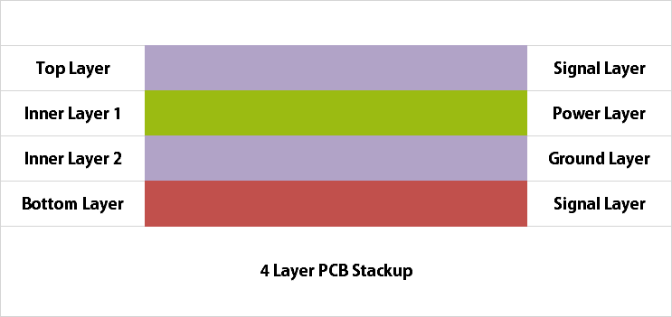
The first type of 4 layer PCB stack up
The bottom layer of the PCB is the key signal layer. Here, core thickness also matters, and it should not be too much. This thickness of the core and PP (prepreg) between the layers is responsible for the distribution impedance. The lesser the distance between power and ground layer, the lesser will be the plane impedance. If the thickness is more, then it would be difficult to decouple the power plane.
2) The Second Type of 4 Layer PCB Stack up:
- Top Layer – Power Layer
- Inner Layer 1- Signal Layer
- Inner Layer 2 – Signal Layer
- Bottom Layer – Ground Layer
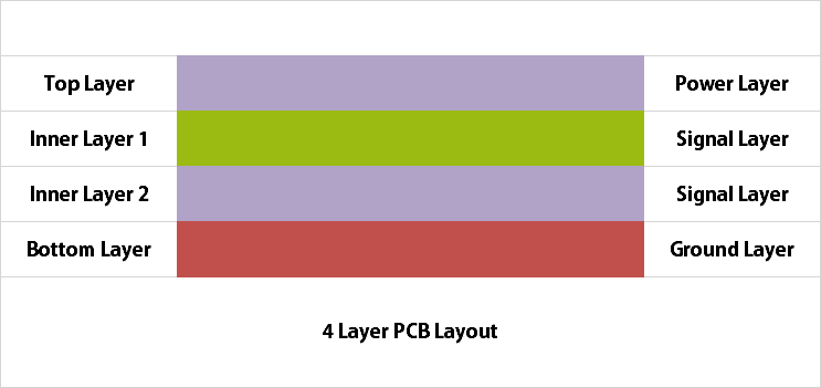
The second type of 4 layer PCB stack up
This stack-up is one of the safest stack-ups for a 4-layer PCB. The power and ground layer act as a shield for the signal layers. But this stack up has some disadvantages.
The first disadvantage is the distance between the power and the ground layer. The plane impedance increases because of the distance between these two. Secondly, due to the effect of electronic components, the reference layer is not complete, so the impedance of the signal is not continuous. Due to a number of components, it is very difficult to use the ground layer as a complete reference layer. Moreover, it isn’t easy to implement as well. But the shielding of the signal layer is excellent in this stack up.
3) The Third Type of 4 Layer PCB Stack up:
- Top Layer – Signal Layer
- Inner Layer 1- Ground Layer
- Inner Layer 2 – Power Layer
- Bottom Layer – Signal Layer
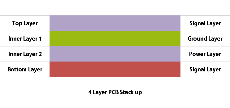
The third type of 4 layer PCB stack up
The third type of stack-up is very similar to the first one. In the first stack up, we know that the main device is connected to the bottom, but not in this stack up. Here, the key signal layer is the top layer. The rest of the stack-up is pretty the same.
Think carefully: What kind of stackup is the best 4-layer PCB stack up?
If you want to know more about other multilayer PCB stack-up, such as 6-layer PCB Stackup/8-layer PCB stack-up, etc., you can click the button below to download the pdf file for reference.
4 Layer PCB Thickness
4 Layer PCB Core and Prepreg (PP) Thickness
There are two types of Core and PP thicknesses when it comes to 4-layer PCBs. The standard one is 1.6 mm, and the others are a bit typical. 1.2mm is also commonly used. In 1.6 mm thick PCB, double side core material consists of 1.2 mm, and the two PP have a thickness of 0.2 mm, which becomes 1.6 mm.
Other typical 1.2mm thickness comprises double-sided core material of 0.8 mm, 0.2 mm PP along with coil, and 0.2 mm PP with copper. These two thicknesses have their own pros and cons, and the choice depends on the user. The cost of a 4-layer PCB also depends on the thickness.
related Reading:
Why Use 4 Layer PCB?
4 Layer PCB Advantages
A 4 layer PCB offers many benefits over a standard double-sided PCB. 4 layer PCB allows for better signal integrity and timing control. Moreover, they also provide increased routing options and improve thermal characteristics. Although 4 layer PCBs are more expensive than their double-layer PCB, the benefits often outweigh the cost.
- Improved signal routing: A 4 layer PCB stackup enables signal routing inside the PCB stackup. The arrangement of layers on a 4 layer PCB stackup can play a significant role in signal routing. A good arrangement enables easier signal routing.
- EMI Shielding: This is another advantage of a 4 layer PCB. Since 4 layer PCB features four layers, it offers better EMI shielding. The ground planes serve as a shield for the inner layers. These planes protect against electromagnetic impedance. They can also prevent any EMI discharges in the circuit.
- Thermal control: A 4 layer PCB stackup offers better thermal control. The design of a 4 layer PCB can distribute warmth throughout the board layer stackup.
- Higher assembly density: These PCBs incorporate four separate layers into one board, increasing the assembly density.
- Smaller and more compact designs: A 4 layer PCB is smaller. This makes it ideal for the production of today’s electronic devices.
What industries are 4-layer PCBs used for?
4 Layer PCB Applications
The emergence of multilayer PCBs has extensively promoted the development of the electronics industry. Due to their more compact design, multilayer PCBs are more suitable for complex applications. People’s demand for high-end electronic products is increasing, and the demand for multilayer PCB is also increasing, and 4-layer PCB has the advantages of multilayer PCB and controllable cost effect. The following are typical applications for 4-layer PCBs.
- Medical equipment: 4-layer PCB boards are widely used in the medical space because of their miniaturized sizes and high functionality. Some medical devices commonly use 4-layer PCBs, including X-ray machines and CT scans.
- Consumer electronics: Consumer electronics have printed circuit boards, but most contain multilayer PCBs instead of single-layer PCBs. These gadgets range from universal TV remotes to intelligent wearables.
- Computer electronics: In the computer world, essential components like motherboards use multilayer boards because of their small sizes and super functionality. In this industry, performance is a preferred trait to cost. Therefore, 4-layer boards are widely used.
- Telecommunications: Telecommunication devices widely use 4-layer PCBs in various applications, like signal broadcast, GPS, and satellite use cases, primarily because they are more durable and highly functional.
- Industrial: The four conductive layers in 4-layer PCBs make them ideal for the use case where rough handling is often experienced, e.g., in industrial controls. These boards are widely applied in the manufacturing process to control machines because of their miniaturized sizes, high durability, and performance.
- Military and defense: Because of their durability, performance, and low-weights, 4-layer PCB boards are widely applied in high-speed military equipment.
- Automotive: This industry has become more reliant on electronics, especially with the invention of electric cars. Electronic devices control GPS, onboard machines, headlight switches, and engine sensors.
- Aerospace: Like the automotive industry, the aerospace sector requires small, high-performing devices.
Generally, 4-layer PCB boards will help you minimize your design, increase its EMI performance, and facilitate complex routing. This is why they are widely applied in almost every industry.
What is the difference between a 4-layer PCB and a double-sided PCB?
2-Layer VS. 4-layer PCB
The first and basic difference between 2-layer and 4-layer PCB is the number of layers, as the name suggests. A 4-layer PCB has two additional layers for power and routing. The signals are usually routed inside the PCB, and the top and bottom layers are used for grounding. But as mentioned earlier, the inner layers are usually used for power and grounding.
In a 4-layer PCB arrangement, routing is much easier than in a 2-layer PCB. Moreover, a 4-layer PCB is more expensive and complex than a 2-layer PCB. The 4-layer PCB must be used when required because it is difficult and inefficient to use a 4-layer PCB for a simpler task, and it will be impractical.
The inner layers of a 4-layer PCB can hide traces that makes debugging extremely difficult. If a 4-layer PCB requires debugging, it would be easy to follow CAD designs and drawings rather than following the traces. But a 4-layer PCB makes your circuit compact and increases its performance. It also makes complex routing easy.
4 Layer PCB Prototype Service
4-layer PCBs are a bit complex; therefore, so you might not get the desired results. It requires the testing of desired results. There could be multiple errors and problems in the first prototype; thus, you might need to revise the design and make other amendments.
Before the mass production of PCBs, it is important to get a prototype. Once you are sure everything is perfect, you can proceed with the batch production. At JHYPCB, we offer quick 4-layer PCB prototypes so that you can test everything on your end. You can even order one 4-layer PCB prototype or as many as you want.
4 Layer PCB Manufacturing
How to Make a 4 Layer PCB?
4-layer PCB manufacturing starts with the inner layers, and for a 4-layer PCB, the second and third circuit layers are the so-called “inner layers.” Below is a standard 4-layer FR-4 PCB manufacturing process.
4 Layer PCB manufacturing process:
- Step 1: Clean in the Chemical Method
- Step 2: Inner Layers Laminate Dry Film
- Step 3: Inner Layers Image Expose & Develop
- Step 4: Copper Etching
- Step 5: Strip Resist
- Step 6: Layer up and Bond with prepreg
- Step 7: Layer up with Copper Foil
- Step 8: Drilling
- Step 9: Plating and Copper Deposition
- Step 10: Outer Layer Imaging
- Step 11: Copper Plating
- Step 12: Tin Plating
- Step 13: Final Etching
- Step 14: Solder Mask
- Step 15: Surface Finish
- Step 16: Silkscreen
- Step 17: Electrical Test
- Step 18: Profiling and V-Scoring
The above steps state how to make a four-layer PCB. 4-layer PCB manufacturing is much more complicated than single-layer or double-layer PCB manufacturing. In addition to cost-effective 4-layer PCB fabrication, JHY provides multi-layer PCB assembly services and free DFM, DFT, and DFX services.
Learn more about How to Build a Multilayer PCB?
4 Layer PCB Price
4 Layer PCB Cost
As discussed above, there are multiple factors on which 4-layer PCB price depends. The type of stack up and the thickness are the most important. The other things that contribute to the price are the material of the PCB, copper thickness, surface finish, Via process, testing, impedance control, etc. The quote of the PCB is determined by looking at all the factors, but you don’t need to worry about these things. You need to provide us with the details, and we will give you a reasonable quote.
- Board Size: As 4 layer PCBs board size varies, the larger 4 layer PCBs will cost more.
- Material: Many materials can be used for 4-layer PCB manufacturing, such as FR-4, High Tg material, and High-frequency material; High Tg material is more expensive than standard FR-4 sheet.
- Complexity: The complexity of 4 layer PCB is reflected in the difficulty of manufacturing. The 4-layer PCB with buried blind holes is more difficult to manufacture, and the price will be higher.
- Copper thickness: Copper thickness is also one of the main factors affecting the price of 4-layer PCB.
- Surface finish: There are a variety of surface finishes available; immersion gold and gold plated are more expensive than OSP or HASL; there’s no question about that.
4 Layer PCB Manufacturer in China
Get Your 4-Layer PCB from JHYPCB
JHYPCB is a well-known service provider of all types of PCB and Assembly services. We offer solutions to all your problems under one roof. We can provide 4-layer PCBs and prototypes at a reasonable price. There is no restriction on the quantity; you can even order one PCB. We will make sure to deliver your PCB as soon as possible.
Our strict quality management system ensures high-quality PCBs. We are RoHS, UL, and ISO certified. Thus, we take responsibility from component procurement to the delivery of PCBs at your doorstep. For more information and details, feel free to contact our 24/7 customer service team.
4 Layer PCB Fabrication Capability
| Provide free DFM Checking, and We can suggest 4 layer PCB stack-up | |
| Copper Thickness | Max to 6 oz inner copper, 12 oz outer copper |
| Min Hole | 0.15mm by mechanical drilling, 0.1mm by laser |
| Board Thickness | 0.4mm – 6.5mm |
| Surface Finish | Immersion gold, Immersion Silver, Immersion Tin, Hard Gold, OSP |
| Soler Mask | Green/Yellow/White/Black/Custom |
| Silkscreen | White/Black/Yellow/Custom |
| Accept 4 layer PCB with Blind or buried Via Hole | |
| 100% Testing | |
| 100% on-time delivery | |
4 Layer PCB FAQs
Most frequent questions and answers
Some people think that the following 4-layer PCB stackup is the best:
1. GND
2. Signals
3. Signals
4. GND
For the following reasons:
1. Signal layers are adjacent to ground planes.
2. Signal layers are tightly coupled (close) to their adjacent planes.
3. The ground planes can act as shields for the inner signal layers. (I think this requires stitching ??)
4. Multiple ground planes lower the ground (reference plane) impedance of the board and reduce the common-mode radiation.
But, I will tell you that there is no best PCB stackup with 4 layer PCB, all is depends on your application.
Both double-sided PCB and 4-layer PCB are commonly printed circuit boards. When to choose a double-layer PCB and when to choose a 4-layer circuit board, this needs to be determined according to different application requirements, including:
1. Since 4-layer PCB has more routing than double-sided PCB, 4-layer PCB can have more functions in a smaller space.
2. If your project is more complex, a 4-layer PCB is required.
3. If your application requires good durability, please choose a 4-layer PCB.
4. If you consider a reasonable budget, it is best to choose a 2-layer PCB.
5. Due to the consideration of delivery time, the delivery time of 2-layer PCB is faster than 4-layer PCB.
In short, you also need to decide whether to choose a double-sided PCB or a 4-layer PCB based on other more situations.
Because 4-layer PCBs have two additional routing layers for signals, which is conducive to the miniaturization of the circuit board and the integration of complex equipment. And 4-layer PCBs are conducive to designers who design for manufacturability.
For details, please refer to the advantages of 4-layer PCB and its application scenarios in this article.
4 layer PCB means there are 4 layers to rout electrical signals: Top Layer, Inner Layer 1, Inner Layer 2 and Bottom Layer.
The price and manufacturing cost of a four-layer PCB depends on the materials used for manufacturing, whether there are special processes such as buried vias, impedance control, etc, quantity, delivery date, and surface treatment process; even different PCB manufacturers have different prices.
Related PCB Board Fabrication Service
Rigid PCB is a Traditional printed circuit board, one of the most used and produced PCBs.

It can realize 3D three-dimensional assembly, which is completely different from rigid PCB.

The excellent combination of rigid PCB and flexible PCB realizes an incredible experience.

Single-sided or single-layer PCB is the simplest circuit board, but they are still widely used.

The 6-layer PCB has more wiring layers, allowing a higher-precision device design.
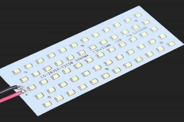
LED PCB boards are widely used in the lighting industry, such as plant growth lights.
Related Posts
- What is a Multilayer PCB and What are the Advantages?
- Angle Control in Multilayer PCB
- Custom Circuit Board Printing
- Top PCB Board Manufacturer And Supplier In China
- The Best And Fastest PCB Manufacturer In China
- Custom PCB Manufacturer In China
- Why Choose Chinese PCB Manufacturer
- How to Store PCB and PCBA?
- What Is FR-4 Material In PCB Fabrication?
- What Are the Multilayer PCB Applications?