Minimizing solder joint defects in PCB assembly should be the goal of all SMT PCB manufacturers.
As a well-known SMT PCB assembler in China, we have provided satisfactory PCB assembly services to customers worldwide. While guaranteeing the delivery time, we are also committed to minimizing all quality defects in PCB assembly. To achieve and maintain the quality of our products, we are constantly summing up and analyzing these defects.
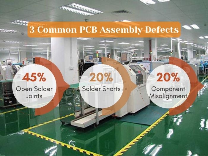
According to industry statistics and our long-term accumulated experience, 60% to 90% of quality defects in SMT PCB assembly are related to solder paste printing, and 75% of soldering defects are mainly reflected in the following three aspects:
Open Solder Joints-35%
Solder Shorts-20%
Component Misalignment-20%
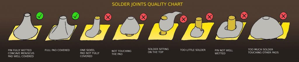
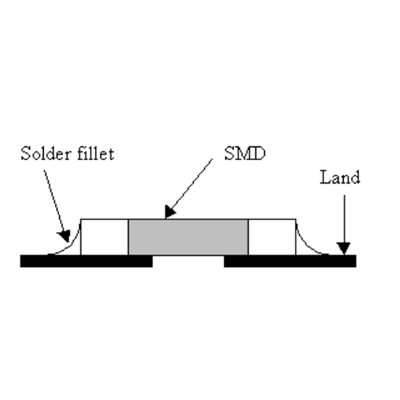
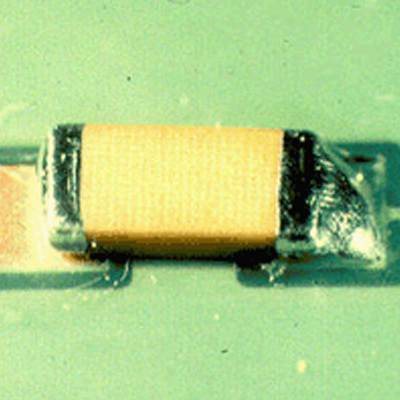
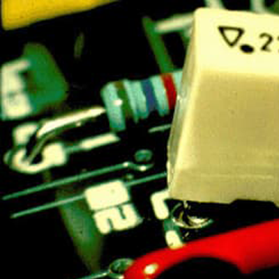
Comparison of ideal solder joint and poor solder joint
We will introduce the following defects in this article:
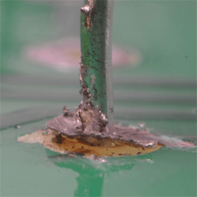
1. False Solder: It seems to be soldered on the surface but not soldered. Sometimes, the leads can be pulled out of the solder joints with toothpicks or tweezers. False welding is somewhat similar to virtual welding; it looks like the welding is on, but sometimes it is OK, and sometimes NG during the test, and the contact is bad.
2. Inveracious solder, or incomplete solder: Incomplete solder is characterized by a rough surface and no gloss, a typical circuit fault. There are two reasons for incomplete solder. One is that there is only a tiny amount of solder at the solder joints caused by improper production technology, resulting in poor contact, which is always on and off. Unveracious solder and False Solder refer to that the surface of the weldment is not fully plated with tin, and the weldment is not fixed by tin. They are all caused by the weldment’s surface not being cleaned or the flux being used too little. Another reason for the incomplete solder is that the electrical appliances have been used for a long time, and some components with severe heat generation have aged and peeled at the solder joints.
3. Empty Solder or Missing Solder: This refers to an SMT defect caused by the lack of tin or other factors between the component lead pin and pad. Empty soldering means that there is tin on the pad, and no tin on the components, resulting in no contact between the two and completely disconnected.
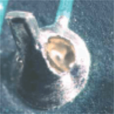
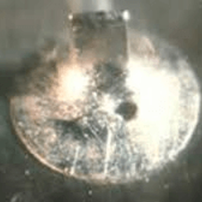
4. Cold Solder: It means that there is no soldering band formed on the soldering interface of the part (that is, the soldering is poor). Too low reflow soldering temperature, short reflow soldering time, and tin-eating properties will cause cold soldering. It can be seen from the color of cold welding that the surface color of the cold solder joints is different from the standard color. The color of the cold solder joints is generally black, and in severe cases, tin beads can be seen.
5. Poor Solder/Solder insufficient
Definition: There is tin soldering between the pins of the component and the PAD, but it does not meet the quality requirements of the soldering standard, which is called more miniature tin.
Impact: The solderability of the component is unreliable, which may cause the component to be soldered weakly or cause circuit failure and affect the board’s function.
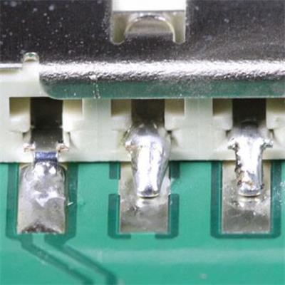
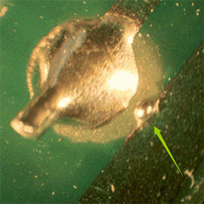
6. Short circuit (Solder Bridge)
Definition: Connecting two independent and adjacent pins together are called a short circuit
Impact: A short circuit will cause different circuits or components to be short-circuited, resulting in excessive current, affecting the normal function of the circuit, and even burning the board.
7. Non-wetting
Definition: The PAD/PIN of the component and the PAD of the PCB board are not soldered well, which is called Non-wetting.
Impact: This leads to a decrease in the reliability of component welding, affects the connection of components and circuits, and affects the board’s normal function.
8. Tombstone
Definition: One end of the part is well welded, and the other is not welded and separated from the PAD of the PCB and stands up, which is called a tombstone.
Impact: The component cannot be appropriately connected to the PCB’s PAD, resulting in an open circuit, which affects the board’s function.
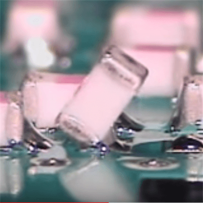
9. Offset
Definition: The PAD/PIN of the component is not aligned with the PAD of the PCB, which exceeds one-half of the width of the part, which is called displacement
Impact: The product’s appearance is affected, and the reliability of the soldering tin of the component is reduced, which may lead to poor electrical properties of the board.
10. Missing
Definition: Where there should be components, but there are no components, it is called missing parts
Impact: lead to an open circuit, affect the board’s function.
11. Extra Part
Definition: The components overlap, or there should not be the component’s position, the component is there, called extra-part.
Impact: affect the product’s appearance; affect the electrical performance of the product; affect the assembly of the board.
12. Sideward
Definition: The welding position of the component is welded on its side, called Sideward.
Impact: Affect the appearance of the product, reduce the welding reliability of components, and affect the assembly of the board.
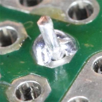
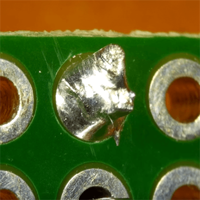
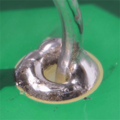
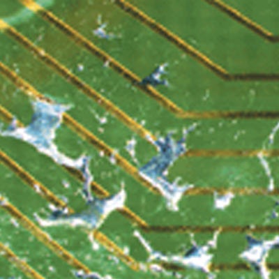
13. Solder Ball/Solder Dreg
Definition: The condensed spherical or irregularly shaped tin remaining on the PCB is called Solder Ball/Solder Dreg.
Impact: Affect the product’s appearance, affect the reliability of the soldering tin of the component, and cause a potential short circuit possibility.
14. Bump
Definition: When the component is impacted by an external force, its solderability is affected, or the component is knocked off. It is called a bump.
Impact: Severely affect the reliability of the soldering tin of the component, resulting in abnormal connection of the circuit.
15. Float
Definition: The phenomenon that components cannot be close to the PCB board during soldering or assembly is called floating.
Impact: The floating height of the Chip components can easily cause collisions, and the floating height of the connector will cause defects in the assembly of the entire product.
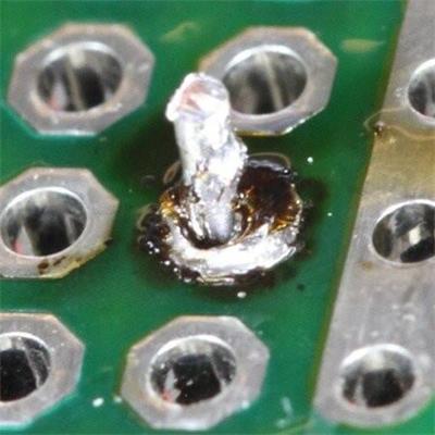
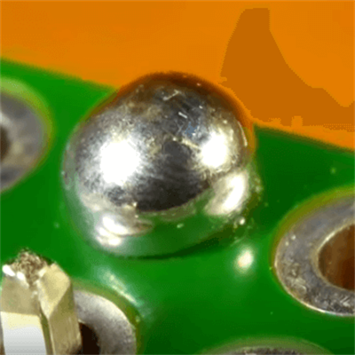
16. Excess Solder
Definition: Too much solder on the component causes the component to be stained, called Excess Solder.
Impact: Affect the appearance of the product, cause potential hazards to the electrical connection of components, and affect the assembly of the board.
17. Reverse
Definition: The component with polarity or direction requirement has the wrong direction or opposite after surface mounting, which is called reverse.
Impact: Severely affect circuit connectivity.
18. Wrong Parts
Definition: The actual component at the component’s position does not match the component required to be mounting, which is called a wrong piece.
Impact: Seriously affect the appearance or electrical function of the product.
19. Oxygenation
Definition: PCB or component solder terminal and component PAD or PCB metal contact part are corroded or discolored by oxygen, called oxidation.
Impact: Affect the appearance of the product, reduce the reliability of the soldering of the components, and the oxidation of the connector’s gold finger will affect the connector’s data connection.
20. Solder Crack or Fractured Solder
Definition: The soldered part is cracked and caused by external force or other stress, called tin crack.
Impact: Severely affect the welding reliability of the components, easily cause open circuits, and affect the electrical functions of the PCB board.
21. Cool Solder
Definition: When the solder passes through the furnace because the temperature does not meet the requirements, the solder does not completely melt and then solidifies, called cold welding.
Impact: Severely affect the solder reliability of the components, and affect the electrical functions of the PCB board.
22. Contamination
Definition: Impurities/soils required for abnormal soldering remaining under the components or on the PCB surface are called foreign objects.
Impact: Affect the appearance of the product and reduce the welding reliability of the component.
23. Warpage
Definition: PCB board bending/deformation caused by incoming materials or SMT process is called board warp.
Impact: Severely affect the product’s appearance, affect the reliability of the solder of the component, and affect the assembly of the finished product.
24. Circuit Defect
Definition: PCB circuit has bad phenomena such as circuit damage, indentation, disconnection due to incoming materials, or SMT process problems, which is called a poor circuit.
Impact: affect the product’s appearance, the reliability of the line, and the regular line connection.
25. Solder Resist Defect
Definition: Too little solder resist oil on PCB board causes the bottom copper to be exposed, or too much solder resists oil, called Solder Resist Defect.
Impact: Affect the product’s appearance; too little solder mask will quickly lead to increased oxidation of the board; too much solder mask will affect the welding quality of the components.
26. Lead Float/Bent
Definition: The component leads are tilted/crooked due to incoming materials, or the lead is tilted/crooked due to external force, called foot tilt/crooked.
Impact: Affect the appearance of the product, reduce the reliability of component welding, and affect the assembly of the product.
27. Gold Finger Touch Solder
Definition: The surface of the gold finger is stained with solder paste for various reasons, which is called the gold finger dip tin.
Impact: affect the appearance of the product, affect the assembly of the golden finger, and affect the normal data transmission of the golden finger.
28. Hole Damage
Definition: PCB board holes are damaged/deformed due to poor incoming materials or SMT process problems, called hole damage/deformation.
Impact: affect the product’s appearance, affect the electrical connection of the hole, and affect the assembly of the product.
29. Damage
Definition: The component body is damaged or cracked due to incoming materials or external force, called a damaged part.
Impact: Affect the component’s appearance, reduce the electrical reliability of the component, and reduce the service life of the component and the board.
30. Solder Fines
Solder Fines refers to the solder powder size balls formed by the metal particles in the solder paste splashing around the connection point during reflow soldering.
Methods to Reduce and Prevent PCB Assembly Defects
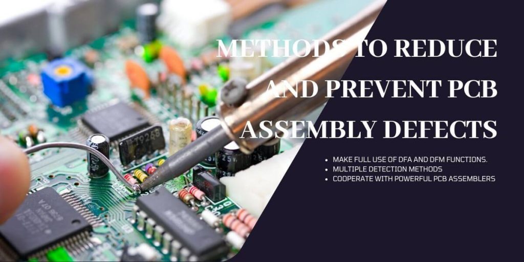
1. Make full use of DFA and DFM functions.
DFA and DFM can detect problems in advance and solve them during the product design stage. This is also the prerequisite for you to get a perfect product.
2. When you place an order with us, we will also provide you with a DFM inspection service before production, and this is free.
3. Multiple detection methods
You can tell us what PCBA inspection items you need. In addition, we will also provide you with comprehensive PCBA inspection services, including visual inspection, AOI and X-ray, etc. Please read the following article to introduce PCB and PCBA inspection items and services.
IPC standard for PCBA
All PCB and PCBA products need to comply with the corresponding IPC standards. To learn more about PCB and PCBA IPC standards, please click here.
Why choose us as your SMT PCB assembler?
1. Strong technical strength
JHYPCB has an advanced SMT factory: JHYPCB has always insisted that advanced productivity is the prerequisite to ensuring product quality. We have high-end SMT machines and various PCBA inspection equipment, including Fuji, Panasonic high-speed placement machines, AOI optical inspection equipment, etc.
Our DIP production line has two large wave soldering machines, which can quickly complete the customer’s DIP assembly tasks.
2. Strong production capacity
We have a daily production capacity of 5 million points. More than 20 skilled front-line employees have worked for more than five years. The highly professional and rich experience of these workers effectively guarantees the quality of customers’ products.
3. Quality Assurance
In addition to advanced production equipment and skilled and experienced workers, each of our processes is equipped with quality control personnel, who will provide a strong guarantee for the quality of your products.
The meticulous and comprehensive inspection will find out all-around product quality defects and correct them in time.
4. Stable delivery cycle
We have cumulatively provided electronic assembly and SMT soldering services to thousands of customers. It is precisely because each of our procedures is carried out in an orderly manner, and we find and solve problems in time, so in the end, we can ensure that our customers can receive their goods in time.
5. Reliable after-sales service
Experienced maintenance engineers can repair various SMT welding defects. At the same time, the product will pass strict quality inspection before leaving the factory to ensure that every circuit board delivered to the customer is perfect. If there is any problem with your order, you will get the fastest response and solution.


