The printed circuit board is an independent module composed of interconnected electronic components found in the electronic devices used daily around us, such as mobile phones, routers, and personal computers, to complex radars, missiles, and satellites. It’s just that the device casing covers its beautiful light, and we often overlook its genius design. Until the equipment fails or needs functional expansion, you can appreciate its beauty when the equipment shell is disassembled.
The History Of Printed Circuit Board
PCB Prehistoric Era
The origin of electronics can be traced back to 1897. Joseph Thomson discovered the existence of electronics. Electronics were developed based on early electromagnetics and electrical engineering. Before the birth of electronics, humans had already done in-depth research on electromagnetic phenomena. A series of physical laws have been established, such as Coulomb’s law, Ampere’s law, Ohm’s law, Lenz’s law, Faraday’s law of electromagnetic induction, etc.
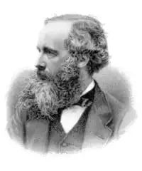
On June 13, 1831, the goddess James Clark Maxwell (June 13, 1831-November 5, 1879) was at 14 India Street in Edinburgh, England. Maxwell is generally considered the physics of the nineteenth century In the family, he had the most significant influence on the tremendous progress of physics at the beginning of the twentieth century. In his thesis “Dynamic Theory of Electromagnetic Fields,” published in 1864, he combined the outstanding achievements of previous electromagnetic studies. He proposed that electric and magnetic fields travel in space in the form of waves at the speed of light. He also proposed that light is an electromagnetic disturbance that causes many electric and magnetic fields phenomena in the same medium. At the same time, theoretically predicted the existence of electromagnetic waves, classified electricity, magnetism, and light as phenomena in the electromagnetic field, proposed the famous Maxwell equations, and established the first complete electromagnetic theory system for electromagnetic production and life. The application has laid a robust theoretical foundation.
Electromagnetism is the most important subject of modern scientific and technological life. Its rapid development has brought humanity into the electrical age and information age. It can be said that without the development of electromagnetics, there would be no modern civilization of humanity; the achievements of this natural science theory laid the foundation for the modern power industry, electronics industry, and radio industry. Of course, there would be no PCB without Maxwell, and there would be no PCB Layout industry.
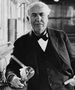
With the support of the electromagnetic theory, people’s use of electromagnetics has reached a certain level. Wired telegraphs and wired telephones have also been invented, and there are telegraphs and telephone lines across the American continent and submarine cables across the Atlantic Ocean. Alexander Graham Bell invented the telephone in 1876, Thomas Edison invented the incandescent lamp in 1879, and Nikola Tesla invented the electric motor in 1888. All of these have prepared sufficient conditions for the birth of electronics.
Two major historical events marked the birth of electronics. One was the discovery of the Edison effect and the verification experiment on the existence of electromagnetic waves.
In 1883, when Edison was working to extend the life of the carbon filament incandescent lamp, he unexpectedly discovered that there was current flowing between the filament and the electrode with positive voltage. When the electrode was negative, there was no current. This is the Edison effect. This discovery led to the invention of the electron tube later.
In 1887, HR Hertz in Germany experimented. He used a spark gap to excite a loop antenna and another loop antenna with a slot to receive it. This confirmed Maxwell’s prediction about the existence of electromagnetic waves. This critical experiment led to later The invention of wireless telegraphy.
The invention of wireless telegraphy was the first outstanding achievement of humanity in using electromagnetic waves. From then on, electronics began a highly prosperous period of research and the use of electromagnetic waves.
Electromagnetic waves are the cornerstone of interconnection and communication between electronic components, and the invention of electronic tubes gave birth to PCBs.
In 1897, German scientist Braun produced the first vacuum tube, and then the vacuum tube period of electronics began. Brown’s vacuum tube is just a prototype of a cathode ray tube (Cathode Ray Tube), which is not very functional.
In 1904, John Fleming of England invented the vacuum diode (diode, also known as a valve at the time), which is composed of a heating filament that emits electrons and a screen that receives electrons; when a positive voltage is applied to the screen, Current will be generated, and no current will be generated when a negative voltage is added.
In 1906, De Forest added a grid to the diode vacuum tube and invented the triode vacuum tube (audion, or triode), which can control the activity of electrons to amplify signals and control electricity. So that the electronic circuit technology has entered the practical application stage. At the same time, it also promoted the development of radio and other electronic industries. In the following 20 years, various electronic devices have continuously emerged. DeForest is also known as the father of radio, the ancestor of television, and the father of electron tubes. “.
The electron tube is the first generation of electronic devices. In the nearly half a century before the invention of the transistor, the electron tube was almost the only electronic device available in various electronic devices. Many subsequent achievements in electronics, such as the invention of television, radar, and computers, are inseparable from the electronic tube. Even in the modern era, when solid-state electronics are very prosperous, vacuum electronics represented by high-power electron tubes (especially microwave power tubes) and electron beam tubes are still an active field.
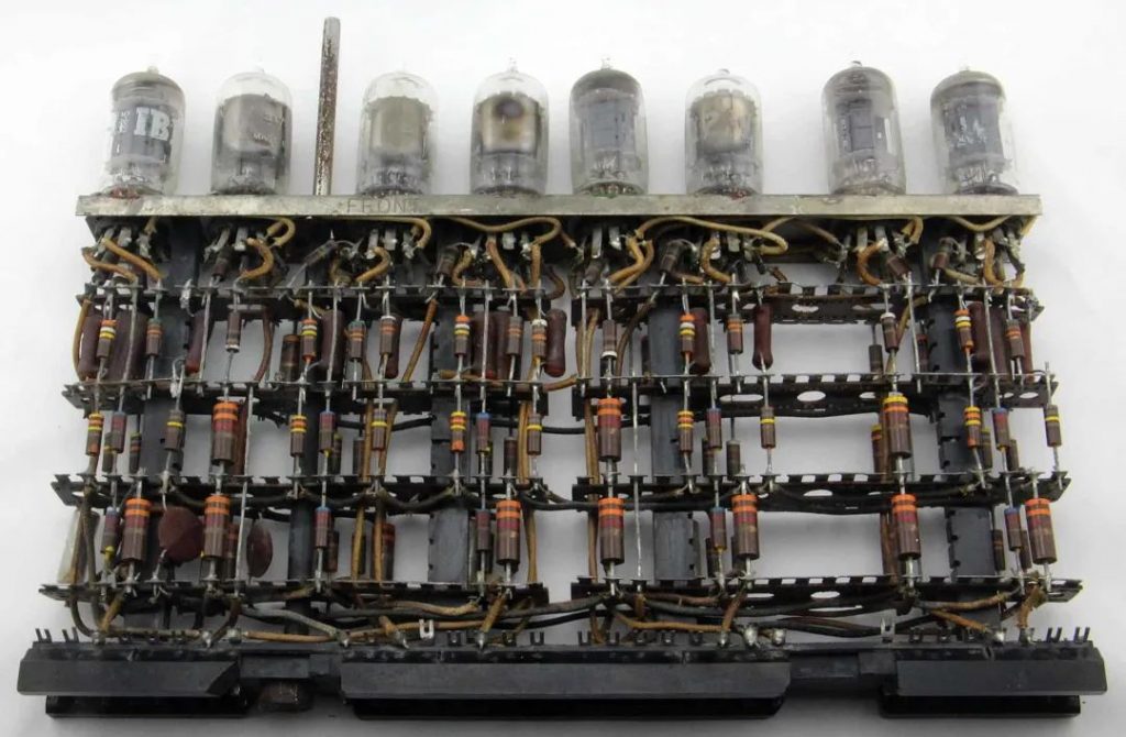
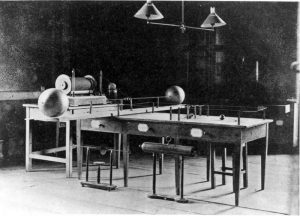
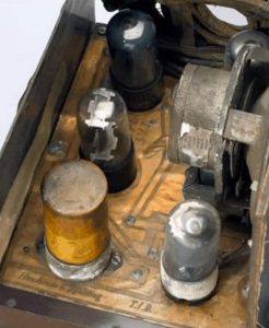
The above picture shows how cumbersome and inefficient it is to produce such an electronic device before PCB technology has been applied on a large scale. A large number of electronic tubes need to use wires coated with insulating resin for manual wiring and soldering between devices, which brings some problems:
- Manual wiring efficiency is low, and there is no way to realize mechanized mass production.
- Manual wiring is prone to installation errors and challenging to check
- The soldering reliability of the terminal is low, and it is easy to loosen and cause poor contact.
To simplify the production of electronic equipment, reduce the wiring between electronic parts, reduce production costs, and improve the reliability of electronic equipment, people have begun to delve into replacing wiring with printing to achieve precise mass production using machines.
The Birth and Development of Printed Circuit Boards
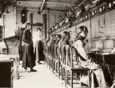
After Faraday published the law of electromagnetic induction in 1831, people began to study how to use electromagnetic principles to realize long-distance communication. Samuel Morse invented the telegraph in 1837, and Bell obtained a patent for the telephone in 1876. By 1904, there were 3 million telephones in the United States that required manual telephone exchange connections.
Printed circuit boards are also developed with the electronic connection system to solve the connection problem of the telegraph/telephone system. In the early days, metal bars or rods connected significant electronic components mounted on wooden bases. Over time, the metal strips were replaced by screw terminals and cables that could be screwed into them to make the connection more flexible, and a metal bottom plate replaced the wooden base. However, with the development of telegraph/telephone services, the number of telephone exchanges has increased, and the electronic operations related to the telephone system have become more complex, requiring a smaller and more compact design.
The "Cradle Period" of Printed Circuit Boards
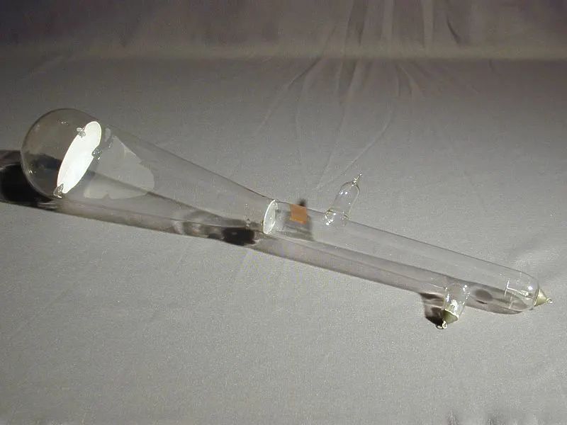
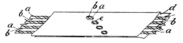
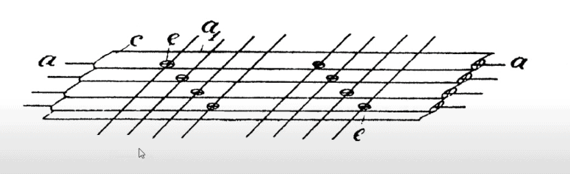
The earliest time point for a patent for PCB-related inventions should be in 1903. A famous German inventor named Albert Hanson applied for a British patent at that time. He pioneered the concept of “wires” Used in the telephone exchange system, and the metal foil is used to cut line conductors. Then paraffin paper is glued on the top and bottom of the line conductors, and via holes are set at the intersections of the lines to realize the electrical interconnection between different layers. This is different from our modern PCB manufacturing method because phenol resin had not yet been invented at that time, and the chemical etching technology is not yet mature. The method invented by Albert Hansen can be said to be the prototype of modern PCB manufacturing.
In 1907, the American chemist Leo Hendrik Baekeland (1863-1944), born in Belgium, improved the production technology of phenolic resin and made the resin practical and industrialized. This has also created necessary conditions for the advent and development of printed circuit boards.
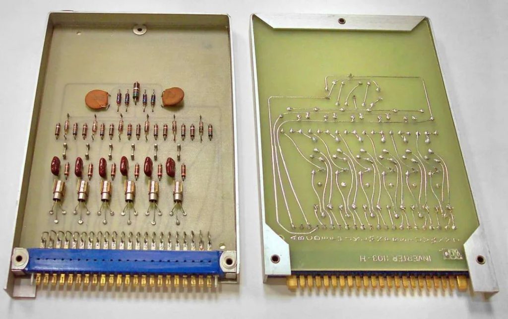
1920s-Early PCB boards are almost everything, from bakelite (the phenolic resin mentioned above, commonly known as bakelite) and turquoise to ordinary old thin wood boards. Some holes can be drilled in the material, and then the flat copper wire can be riveted to the material. The appearance may not look very beautiful, but the idea of later printed circuit boards was born from here. At the time, these circuit boards were mainly used for radios and phonographs.
The Invention of the Printed Circuit Board
Remember the Hertz mentioned above? After Hertz confirmed Maxwell’s prediction of electromagnetic waves through experiments in 1887, by the 1920s, radio had attracted worldwide attention. Moreover, the tube technology is mature enough to start radio broadcasting, and radio will soon be introduced to every household. How to quickly manufacture radios also promotes the evolution of printed circuit board-related technologies.
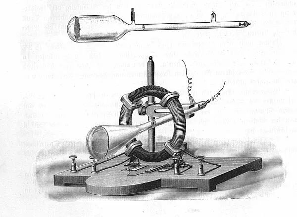
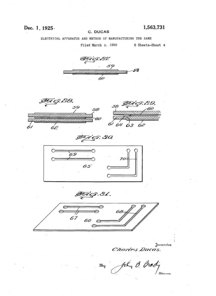
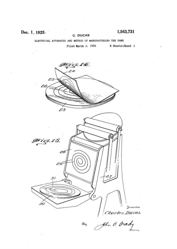
In 1925, Charles Ducas of the United States printed circuit patterns on an insulating substrate and then used electroplating to establish conductors for wiring successfully. At this time, the term “PCB” was born. This method makes it easy to manufacture electrical appliances.
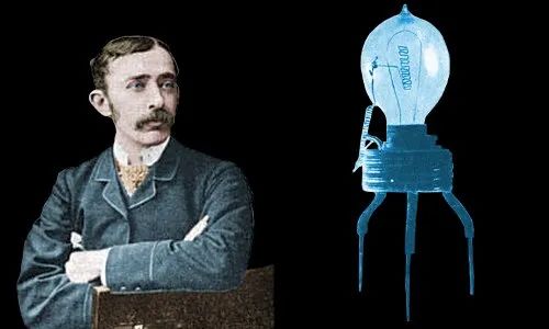
In 1936, the Austrian Dr. Paul Eisler published foil technology in the United Kingdom. He used a printed circuit board in a radio device; also, in 1936, Miyamoto Yoshinosuke of Japan successfully applied for a patent using the spray-attached wiring method. Of the two, Paul Eisler’s method is the most similar to today’s printed circuit boards. This type of method is called subtraction, which removes unnecessary metal. However, Charles Ducas and Miyamoto Kinosuke’s method adds only the required wiring, which is called the additive method.
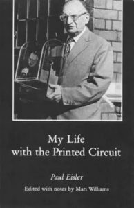
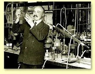
Paul Eisler is also known as the “father of printed circuits.” Still, because the electronic tube components generated a lot of heat and were bulky and inconvenient to install on a printed circuit board, Paul Eisler’s major invention was not paid attention to by the United Kingdom at that time. In the United States, PCB manufacturing technology is only applied to military products.
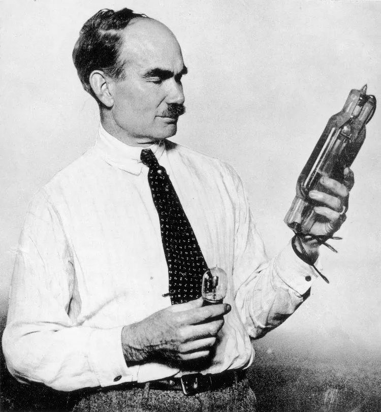
By 1942, Dr. Paul Eisler continued to improve his PCB production method, invented the world’s first practical double-sided PCB, and officially produced it in Pye. The patent application was approved in 1943.
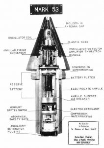
Around 1943, the United States began to use Paul Eisler’s technological invention on a large scale to make proximity fuzes for use in World War II. At the same time, the technology is widely used in military radios.
In 1947, epoxy resin began to be used for manufacturing substrates. At the same time, NBS began to study the manufacturing technology of forming coils, capacitors, and resistors with printed circuit technology.
In 1948, the United States officially recognized the invention of printed circuit boards for commercial use.
However, in the 1950s, there were few electronic devices using PCBs. For example, in the picture on the right, the TV produced by Motorola in 1948 still has no PCB. Good guy, there are all electron tubes densely packed, so if you repair the machine at that time, it would be a daunting expression. If you now own a working Motorola tube TV, how much is it worth? In 1948, all the people who could afford TV were the rich.
Printed Circuit Board Spring
From the 1950s to the 1990s. This is the stage where the PCB industry is formed and rapidly growing, that is, the early stage of PCB industrialization, at which time PCB has become an industry.
After 1948, the United States officially recognized the PCB as an invention for commercial use, which meant that PCBs began to be commercialized on a large scale from military applications.
With the development of electronic technology, in December 1947, a research team composed of Shockley, Barding, and Bratton of Bell Labs in the United States developed a transistor. Transistors with lower heat generation and smaller volume have replaced electron tubes in a large number since the 1950s, creating conditions for the widespread use of printed circuit board technology.
In 1950, a Japanese company tried to coat silver on a glass substrate and copper foil as a conductor on a phenolic resin paper substrate. Beginning in 1950, printed circuit manufacturing technology began to be widely accepted. At this time, etching played a leading role. As transistors became practical, single-sided PCBs made by metal foil etching were successfully developed in the United States and quickly obtained industrial applications.
In 1951, polyimide material was born.
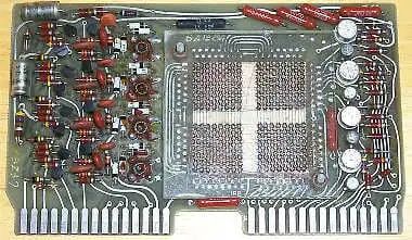
In 1953, Motorola developed a double-sided board with electroplated vias. Around 1955, Japan’s Toshiba Corporation introduced a technology to generate copper oxide on the surface of copper foil, and copper-clad laminates (CCL) appeared. These two technologies were later widely used in the manufacture of multilayer printed circuit boards, and they contributed to the emergence of multilayer printed circuit boards. Since then, multilayer PCBs have been widely used.
In the 1960s, 10 years after printed circuit boards were widely used, PCB technology became increasingly mature. Since the advent of Motorola’s double-sided boards, multilayer printed circuit boards have begun to appear, increasing the ratio of wiring to substrate area.
Printed Circuit Boards Are Already Essential
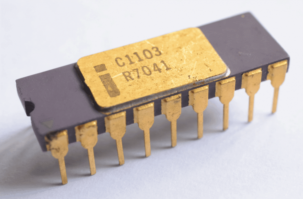
1958: Robert Noyce of Fairchild and Kilby of Texas Instruments respectively invented integrated circuits within a few months, creating the history of microelectronics in the world.
In the 1960s, multi-layer (4+layers) PCBs began to be produced. The plated through-hole metalized double-sided PCB has achieved mass production.
1964: Intel Moore proposed Moore’s Law, predicting that transistor integration will double every 18 months.
1971: Intel introduced 1kb dynamic random access memory (DRAM), marking the emergence of large-scale integrated circuits.
1971: The world’s first microprocessor 4004 was launched by Intel, using MOS technology, which was a milestone invention.
With the large-scale application of integrated circuits, if printed circuit boards are not used in the production of electronic products, the production will bring big troubles.
In the 1970s, multilayer PCBs developed rapidly. They continued to develop in the direction of high-precision, high-density, fine-line small holes, high reliability, low-cost, and continuous automated production to adapt to the pace of Moore’s Law.
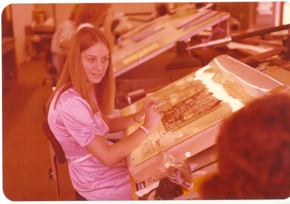
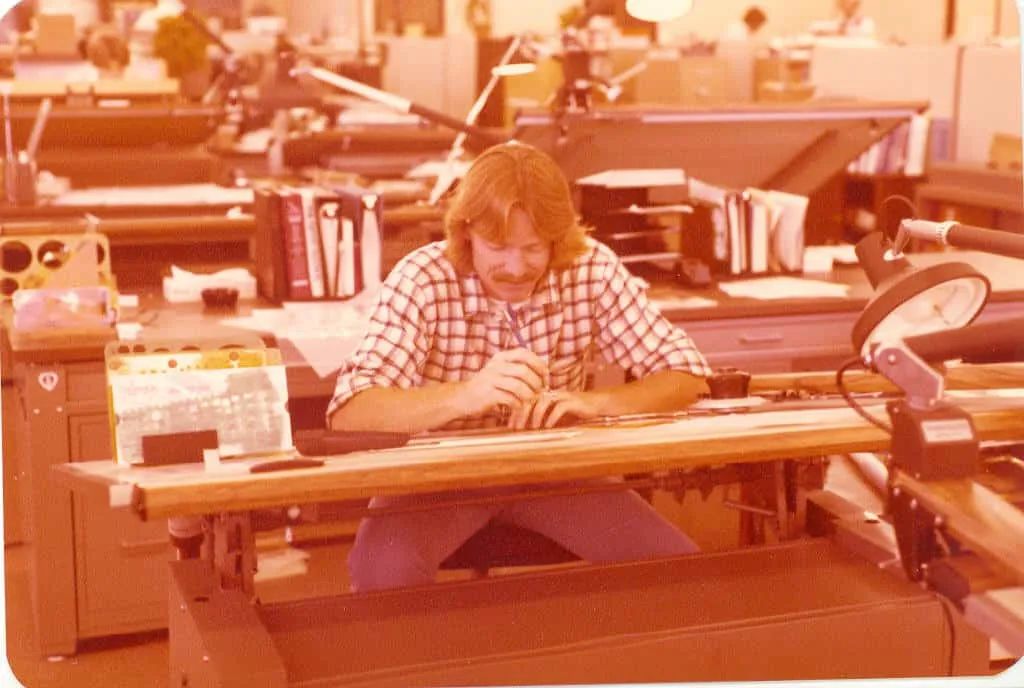
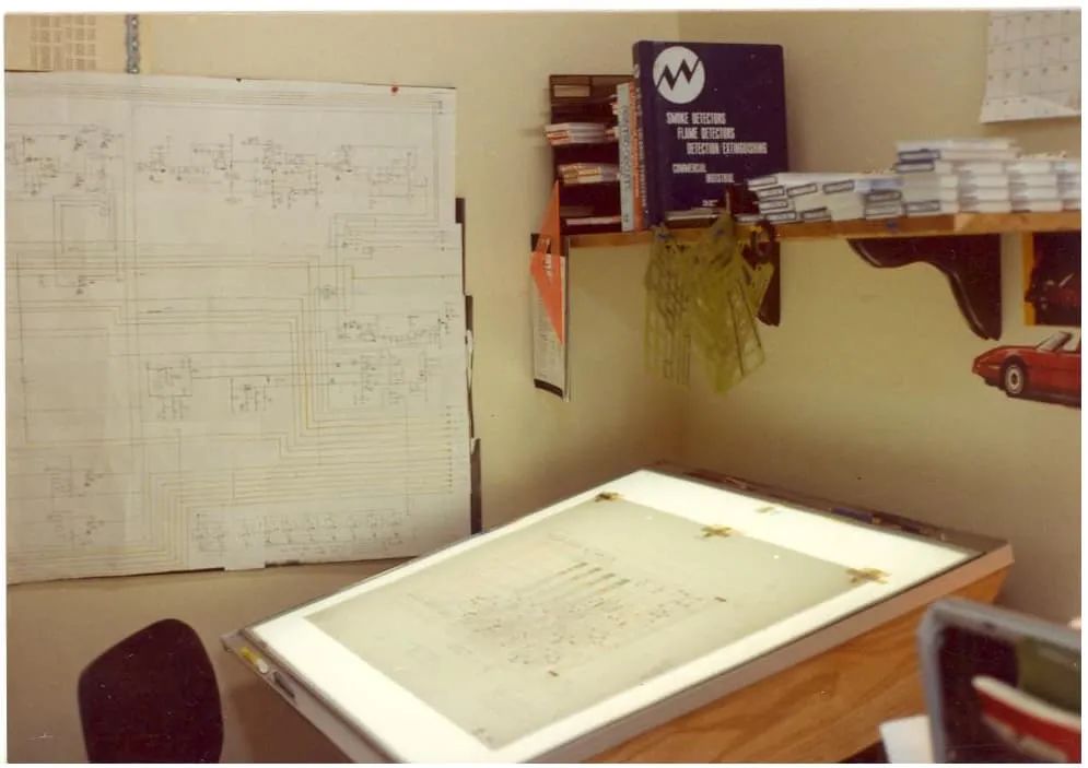
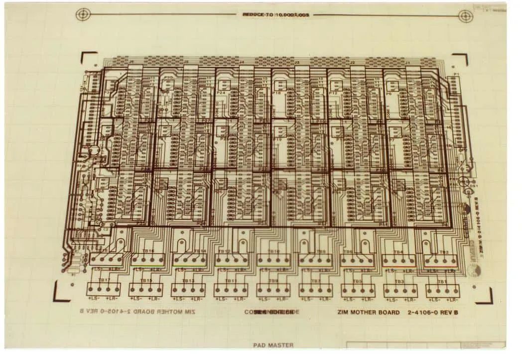
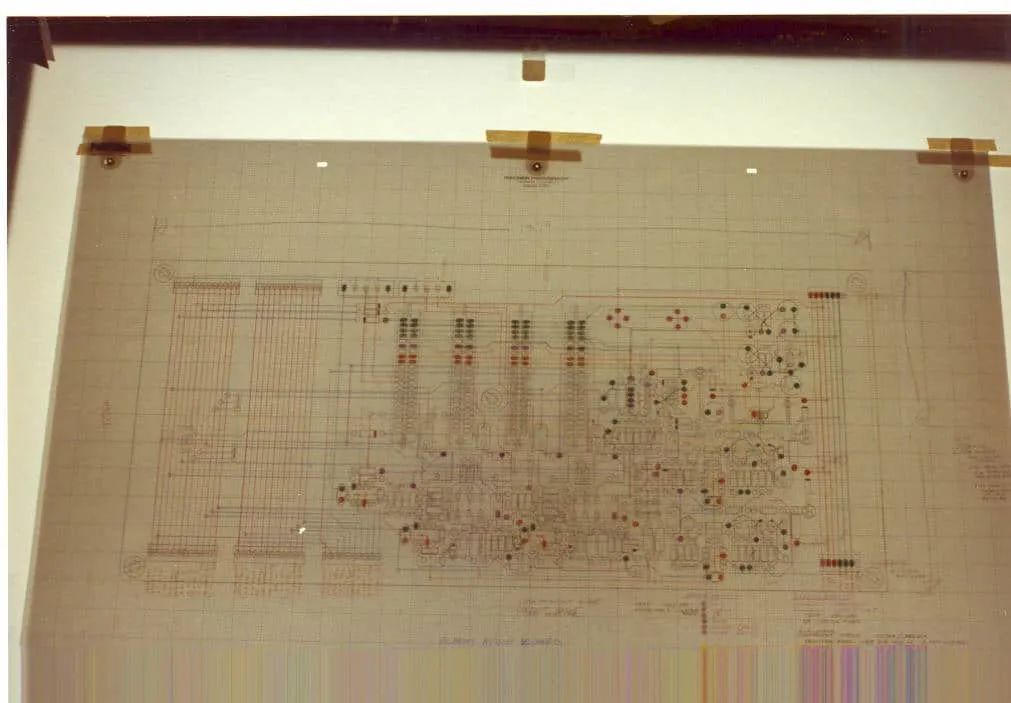
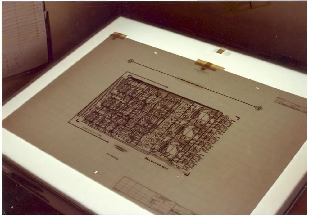
Although the multilayer PCB began to develop rapidly in the 1970s, the PCB design work at that time was still done manually.
At that time, PCB Layout engineers used colored pencils and rulers to draw circuits on transparent polyester film. There were packaging templates and circuit templates for some standard devices to improve drawing efficiency.
In the 1980s, surface mounting technology began to replace through-hole mounting technology to become the mainstream gradually, and it also began to enter the digital age. With the development of electronic devices such as personal computers, optical discs, cameras, game consoles, walkmans, etc., significant changes have taken place in how we consume media.
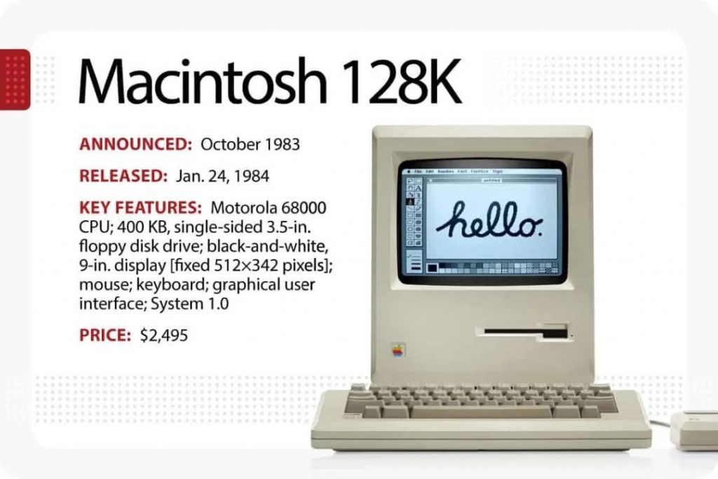
Microsoft released the MS-DOS 1.0 system in 1981, and in 1984 Jobs’ Apple released the Macintosh Macintosh computer (more commonly referred to as Mac). Lenovo was founded in 1984 and began to assemble personal computers. Personal computers began to spread. DOS CAD software began to appear and developed rapidly.
The advent of CAD software has improved the drawing efficiency of designers, and at the same time, improved the reuse rate of PCB design, saving repetitive design time. After the PCB design is completed, directly export the Gerber file and input it into the light painting equipment. At the same time, PCB manufacturing has also begun to use a large number of machinery instead of labor, and PCB production efficiency has improved. PCBs that previously took several weeks to be delivered can now be delivered in a few hours at the earliest. At this time, quick turn PCB factories began to appear.
Since the 1990s, the PCB industry has begun to mature.
In 1993, Paul T. Lin of Motorola applied for a BGA (Ball Grid Array) packaging patent, which marked the beginning of organic packaging substrates.
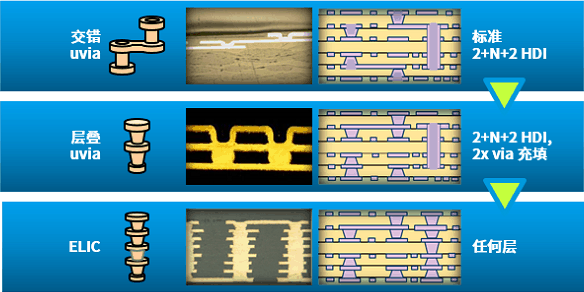
In 1995, Panasonic Corporation developed the BUM PCB manufacturing technology of ALIVH (through-hole between arbitrary layers) structure. This also means that PCB has begun to enter the era of HDI high-density interconnection.
In the early 2000s, PCBs became smaller and more complex. 5-6 mil line width/line spacing is already conventional. High-end PCB board manufacturers have begun to manufacture circuit boards with 3.5-4.5 mil line width/line spacing.
At the same time, flexible PCBs have become more common.
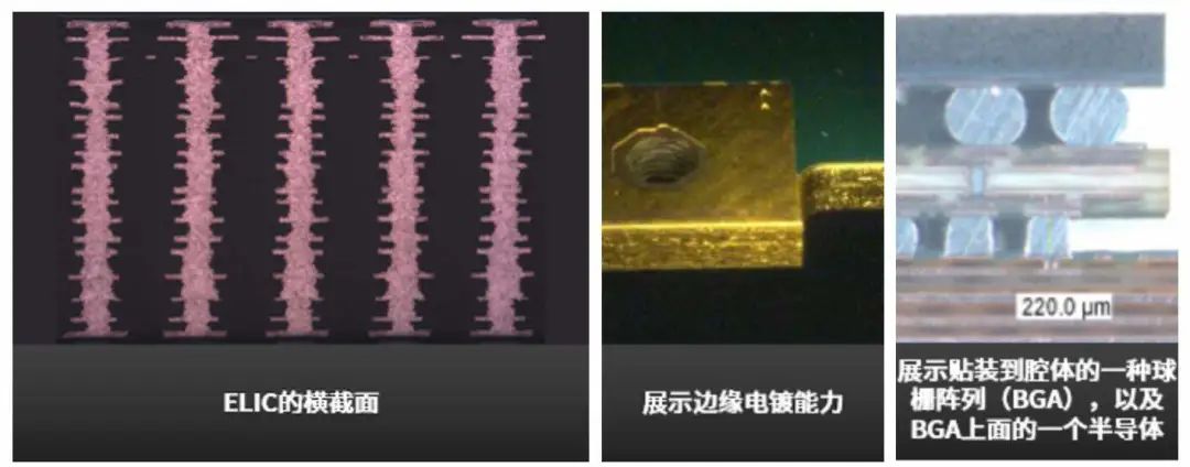
In 2006, the Every Layer Interconnect (ELIC) process was developed. The process uses stacked copper to fill microvias and connect through each circuit board layer. This unique process enables developers to establish a stacked connection between any two layers in the PCB. Although this process increases flexibility and enables designers to maximize interconnect density, ELIC PCB was not widely used until the 2010s.
The development of smartphones, driving the development of HDI PCB technology.
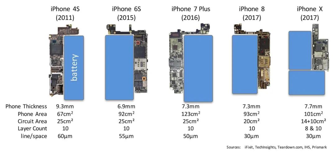
The evolution of smartphones
With the development of smartphones, the second generation of HDI came into being at the beginning of the 21st century. While retaining the laser-drilled micro vias, stacked vias began to replace the staggering vias. Combined with “any layer” construction technology, the final line width/line spacing of the HDI board reached 40μm.
This arbitrary layer method is still based on a subtractive process, and it is inevitable that most high-end HDI still use this technology for mobile electronic products. However, in 2017, HDI began to enter a new stage of development, beginning to shift from a subtractive process to a process based on pattern plating.
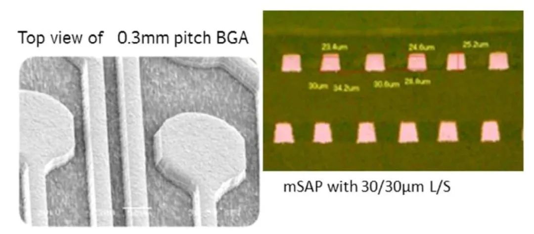
For example, in a 0.3 mm pitch BGA design, there are two traces between the BGA pads. The through-hole size is usually 75 microns, and the pad size is 150 microns. The layout design requires a line width/line spacing of 30 µm/30 µm. Using the existing subtractive process to realize this fine-line structure is very challenging. Etching ability is one of the critical factors, and the finished copper thickness and plating uniformity need to be optimized with the imaging process. This is why the PCB industry now adopts the mSAP process. The mSAP process can quickly produce circuits with optimized conductor shapes compared to the subtractive process. On the entire PCB panel, the width of the upper end of the PCB etching end is almost equal to the width of the lower end. -The line shape is easy to control. Another advantage of mSAP is the use of existing resources and technology, standard PCB technology, such as drilling, electroplating, etc., and the use of traditional materials so that there is good adhesion between the copper and the dielectric layer to ensure the final product High reliability.
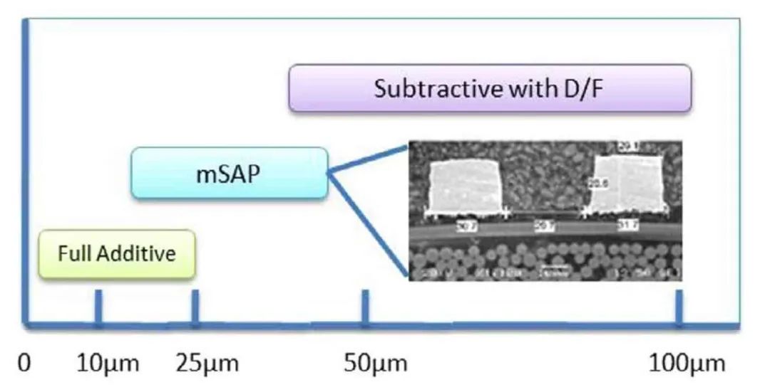
The semi-additive method (mSAP) and the improved semi-additive method (amSAP) are modified and advanced modified versions. They are now expected to become the main processes used in the next generation of HDI PCBs.
Next-generation HDI process
Due to miniaturization, HDI and micropores provide a considerable boost for high density. These technologies will continue to develop with the geometry of the IC unit and become smaller. So the next revolution will be in the field of optical conductors.
With the continuous improvement of VLSI technology, the processor performance of computer systems has improved. However, current electronic computers still use traditional copper wires to connect chip-chip, processor-processor, circuit board-circuit board. The International Semiconductor Technology Blueprint (ITRS) has pointed out that the interconnection between chips will limit the future electronic system because the main problems faced by the copper wire currently used are:
(1) High-speed signal distortion and limited bandwidth;
(2) The transmission loss of metal wires increases with the increase of signal frequency, which limits the transmission distance of high-frequency signals;
(3) It is vulnerable to electromagnetic interference;
(4) High power consumption, etc.
And optical communication has many advantages that traditional electrical signals do not possess, such as high bandwidth, low loss, no crosstalk, anti-electromagnetic interference, etc. Optical fiber has wholly replaced traditional copper wire for long-distance communication for decades. The future development trend is that the communication distance of optical interconnection will gradually become shorter, from the long-distance communication between countries to the signal transmission inside the chip.
At present, the industry generally believes that when the single-channel rate reaches 25 Gb/s or more, electrical interconnection will face significant technical implementation and cost comparison challenges. Therefore, to overcome the “bottleneck” of electronic computers, changing the traditional interconnection methods based on copper wires is necessary. The introduction of optical technology into electronic systems and the replacement of traditional electrical interconnections with new optical interconnections can significantly increase the operating speed of computers and promote the development of high-speed information communication networks, thereby meeting the needs of social development.