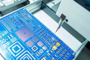
Rigid PCB Fabrication Capability
The continuous upgrading of the process manufacturing capacity is our most competitive advantage. The upgrading of manufacturing capacity also means providing customers with the most advanced production technologies and reducing costs for customers.
Home » PCB Manufacturing Capabilities » Rigid PCB Fabrication Capability
| NO. | Item | Manufacturing Capability |
|---|---|---|
| 1 | PCB Layers | 1~64 Layer |
| 2 | Quality Grade | IPC Class 2|PC Class 3 |
| 3 | Laminate/Base material | FR-4|S1141|High Tg|PTFE|Ceramic PCB|Polyimide|S1000-2|IT180A|Isola-FR408HR|FR406|Isola 370 HR|Rogers|Taconic|Arlon|Halogen Free, etc. |
| 4 | Brand of Laminate | Kingboard|ITEQ|Shengyi|Nanya|Isola|TUC|SYL|Arlon|Nelco|Taconic|Hitachi|Rogers, etc. |
| 5 | High Temperature Material | Normal Tg: Shengyi S1141|KB6160|Huazhen H140(not suitable for lead-free process ) Middle Tg: For HDI、multilayers: SY S1000H|ITEQIT158|HuazhengH150|TU-662|SY S1150G|HuazhengH150HF|H160HF; High Tg: For thick copper、high layer: SY S1000-2|ITEQIT180A|HuazhengH170|ISOLA: FR408R|370HR|TU-752|SY S1165 |
| 6 | High Frequency Circuit Board Material | Rogers|Arlon|Taconic|SY SCGA-500|S7136|HuazhengH5000 |
| 7 | High Speed PCB Material | SY S7439|TU-862HF|TU-872SLK|ISOLA: I-Speed, I-Tera@MT40|Huazheng:H175|H180|H380 |
| 8 | Ink | Taiyo INK (Japan)|KUANGSHUN(China)|RONGDA(China)|Coates Screen(UK)|S.M Materials(Taiwan, China) |
| 9 | Heat Conductivity for Alu. Boards | 1.0 |
| 10 | Chemical | Rohm&Haas (US)|Atotech (Germany)|Umicore (Germany) |
| 11 | PCB Type and Services | Prototype PCB|Rigid PCB|Flexible PCB(FPC)|Rigid-Flex PCB|HDI PCB|High Tg PCB|BGA PCB|Impedance Control PCB|IMS PCB(LED PCB Board, Aluminum PCB, Metal Core PCB)|Multilayer PCB|PCBA(PCB Assembly Service) |
| 12 | Max Board Size | 609 * 889 mm |
| 13 | Board Thickness | 0.1~8.0mm |
| 14 | Board Thickness Tolerance | ±0.1mm / ±10% |
| 15 | Min base copper thickness | Outer layer:1/3oz (12um) ~10oz|Inner layer:1/2oz~6oz |
| 16 | Max finished copperthickness | 6 OZ |
| 17 | Min Mechanical Drilling Hole Size | 6mil(0.15mm) |
| 18 | Min Laser Drilling Hole Size | 3mil(0.075mm) |
| 19 | Min CNC Drilling Hole Size | 0.15mm |
| 20 | Hole Wall Roughness(Max) | 1.5mil |
| 21 | Min trace width/spacing(Inner Layer) | 2/2mil(Outer layer:1/3oz,Inner layer:1/2oz) (H/H OZ base copper) |
| 22 | Min trace width/spacing(Outer Layer) | 2.5/2.5mil (H/H OZ base copper) |
| 23 | Min spacing between hole to inner layer conductor | 6mil |
| 24 | Min spacing between hole to outer layer conductor | 6mil |
| 25 | Min annular ring for via | 3mil |
| 26 | Min annular ring for component hole | 5mil |
| 27 | Min BGA diameter | 8mil |
| 28 | Min BGA pitch | 0.4mm |
| 29 | Min Finished hole size | 0.15mm(CNC)|0.1mm(Laser) |
| 30 | Half Hole Diameter | Minimum Half hole Diameter: 1mm, Half hole is a special technology, so half hole diameter should be greater than 1mm. |
| 31 | Hole Wall Copper Thickness (Thinnest) | ≥0.71mil |
| 32 | Hole Wall Copper Thickness (Average) | ≥0.8mil |
| 33 | Minimum Air Gap | 0.07mm(3mil) |
| 34 | Fine SMD Pitch | 0.07mm(3mil) |
| 35 | Max aspect ratios | 20:1 |
| 36 | Min soldermask bridge width | 3mil |
| 37 | Soldermask/circuit processing method | Film|LDI |
| 38 | Min thickness for insulating layer | 2mil |
| 39 | HDI & special type PCB | HDI(1-3 steps)|R-FPC(2-16 layers)|High frequency mix-pressing(2-14 layers)|Buried capacitance & resistance … |
| 40 | Max. PTH (Round Hole) | 8mm |
| 41 | Max. PTH (Round Slot Holes) | 6*10mm |
| 42 | PTH Deviation | ±3mil |
| 43 | PTH Deviation (Width) | ±4mil |
| 44 | PTH Deviation (Length) | ±5mil |
| 45 | NPTH Deviation | ±2mil |
| 46 | NPTH Deviation (Width) | ±3mil |
| 47 | NPTH Deviation (Length) | ±4mil |
| 48 | Hole Position Deviation | ±3mil |
| 49 | Character Types | Serial Number|Barcode|QR Code |
| 50 | Min Character Width (Legend) | ≥0.15mm, Characters width less than 0.15mm will be unidentifiable. |
| 51 | Min Character Height (Legend) | ≥0.8mm, Characters height less than 0.8mm will be unidentifiable. |
| 52 | Character Width to Height Ratio (Legend) | 1:5, 1:5 is the most suitable ratio for production. |
| 53 | Distance between Trace and Outline | ≥0.3mm(12mil), Ship as individual boards: Distance between Trace and Outline ≥0.3mm, Ship as Panelized boards with V-cut: Distance between Trace and V-cut line ≥0.4mm |
| 54 | Panelization without Spacing | 0mm, Ship as Panelized boards and the spacing between boards is 0mm. |
| 55 | Panelization with Spacing | 1.6mm, Make sure the spacing between boards should be ≥1.6mm, otherwise it will be hard to process routing. |
| 56 | Surface Finishes | OSP|HASL|HASL Lead-Free (HASL LF)|Immersion Silver|Immersion Tin|Plated Gold|Immersion Gold(ENIG)|ENEPIG|Golden Finger+HASL|ENIG+OSP|ENIG+Golden Finger|OSP+Golden Finger, etc. |
| 57 | Solder-Mask Finishing | 1). Wet Film (LPI Soldermask) 2). Peelable Soldermask |
| 58 | Solder Mask Colors | Green|Red|White|Black, Blue|Yellow|Orange|Purple, Gray|Transparent .etc. Matte: Green|Blue|Black, etc. |
| 59 | Silkscreen Colors | Black|White|Yellow, etc. |
| 60 | Electrical Testing | Fixture / Flying Probe |
| 61 | Other Testing | AOI, X-Ray(AU&NI), Two-dimension Measurement, Hole Copper Instrument, Controlled Impedance Test(Coupon test&Third Party Report), Metalloscope, Peeling Strength Tester, Solderability Test, Logic Contamination Test |
| 62 | Profile | 1). CNC Routing (±0.1mm) 2). CNC V-Cut(±0.05mm) 3). Bevelling 4). Mould-Die Punching(±0.1mm) |
| 63 | Special Capabilities | Thick Copper, Thick Gold(5U”), Gold Finger, Blind and Buried Hole, Countersink Hole, Semi-hole, Peelable Mask, Carbon Ink, Counter sink hole, Plated board edge, Press fit hole, Control depth hole, VIA in PAD, Non-conductive resin plug hole, Plating plug hole, Coil PCB, Super Mini PCB, Peelable Mask, Controlled Impedance PCB, etc. |
JHYPCB is a Rigid PCB, Flexible PCB, and Aluminum PCB manufacturing expert; we have been committed to providing customers with low-cost, fast delivery, high-quality products, and services. If you have any questions, please email us at sales@pcbjhy.com.
