
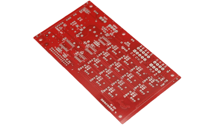
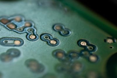
Impedance Control PCB Fabrication
Home » PCB Manufacturing » Impedance Control PCB
With the advancement in technology, it is desired to achieve faster signal processing without distortion and loss in the signal. Conventional PCBs cannot deal with high-speed signals, and the signal received at the receiver end is distorted or has some errors. The issue arises when we deal with high-frequencies, so there is a need for a special PCB that can transmit high-frequency signals with minimum or no distortion. This is where the impedance control PCB comes into play. Impedance Control PCBs have made the transmission of high-frequency signals possible.
PCB Manufacturing Impedance Control: Everything You Must Know
What Is PCB Impedance?
What is Impedance?
Impedance refers to the sum of electric resistance, inductive reactance, and capacitive reactance. While talking about DC signals, there are no inductive reactance and capacitive reactance because these depend on the frequency of the signal, and the frequency of DC is zero. Thus, there is no reactance for DC signals, and the only thing that matters is resistance.
In the case of AC signals, we need to consider electric resistance, inductive reactance, and capacitive reactance. The impact of electric resistance is not affected by frequency, but the inductive reactance and capacitive reactance change with the frequency, and their impact is significant when the frequency is high. Thus, while dealing with high-frequency signals, we need to consider and control impedance to get the desired results.
The Difference Between Impedance And Resistance.
| Resistance | Impedance |
|---|---|
| R | Z |
| Two or more resistances in a series can be added arithmetically. | Vector addition should be performed to sum up the impedances. |
| Unaffected by the supply frequency. | It mainly depends on supply frequency. |
| Current through resistance is always in phase with the voltage across it. | Current and voltage are out of phase. The phase difference depends on the inductance or capacitance present in the impedance. |
Definition & Types of Characteristic Impedance
At a specific frequency, the resistance of a high-frequency signal or electromagnetic wave in the propagation of a signal line of an electronic device relative to a specific reference layer is called a characteristic impedance, which is an electrical impedance, an inductance, resistance, capacitance resistance… a vector sum.
The characteristic impedances commonly found on Impedance Control PCBs are single-ended impedance, differential impedance, and coplanar impedance.
- Single-ended impedance refers to the impedance measured by a single signal line.
- Differential Impedance: Refers to the impedance tested in two equal-width, equally spaced transmission lines for differential driving.
- Coplanar impedance: The impedance measured when the signal line is transmitted between GND / VCC (signal line to its GND / VCC spacing is equal).
What is an Impedance Control PCB?
An impedance control PCB is a special PCB that has calculated impedance according to the requirement. In such PCBs, the desired impedance is maintained so that they can offer the desired results. Conventional PCBs do not have any restriction on impedance, so they cannot be called impedance control PCBs.
The transmission of high-frequency signals is affected by impedance, so it is important to have control over it. Such PCBs can deal with high-frequency signals and prevent distortion and errors during transmission.
There are two ways to control the impedance of the PCB. You can either fix the dielectric thickness of the PCB or mention the impedance in Ohms. Fixing the dielectric thickness is a bit difficult, and you might not get the desired results as the impedance depends on many factors. The best way is to select the desired impedance in Ohms and inform the PCB manufacturer. Now, it is the responsibility of the manufacturer to provide the desired impedance with a tolerance of ±10 Ohms. However, the manufacturer might require some changes in the design or dimensions to ensure the required impedance, and in this case, the manufacturers discuss everything with the buyer before taking any step.
Importance Of Impedance Control
Why Focus on Impedance Control?
If a product needs a specific impedance to operate perfectly, controlled impedance is the way to go. PCBs in high-frequency devices need equal impedance across the entire board to maintain a signal and not damage any data. More adaptation is needed for a higher frequency. Failure to control impedance at this level can increase the switching time on a circuit and lead to errors.
Calculating uncontrolled impedance when the components are placed on a PCB is challenging. This is because components have different tolerances depending on their material, etc. Moreover, component specification is also affected by temperature variations, resulting in product malfunction. You may think that replacing a component is the best step, but that one unsuitable trace is responsible for the real nuisance.
This is why it is essential to measure the impedance of each trace before the PCB design is finalized. The hand-in-hand coordination of designers and manufacturers can make a PCB compliant with appropriate values.
When to Use Controlled Impedance?
Controlled impedance should be considered when a signal must have a particular impedance at high frequencies to function correctly. In high-frequency products, it is essential to match the impedance of PCB traces to maintain data integrity and signal clarity. If the impedance does not match the components’ characteristic impedance, the switching time may be increased, and the circuit may meet random errors.
Why Impedance Control PCB?
This question tickles the mind of beginners that do not know much about PCBs. We need to understand why there is any need for such a PCB.
Impedance control PCBs can provide a safe path that other PCBs cannot provide for high-frequency signals. The most important thing in a high-frequency signal is Signal Integrity, which means the ability to retain the signal in its original shape during transmission. If the signal at the receiver end is nearly the same as at the sender end, then there is signal integrity. It gives a measurement of signal distortion.
While talking about high-frequency signals, signal integrity becomes more important. It is because these signals carry a message which is created using amplitude or frequency modulation. The message is hidden in the signal and decoded at the receiver ends. But if there is any change in the signal, such as a change in frequency and amplitude, then the signal at the receiver end will not be the same as the sender end. It will change the information or message conveyed.
Moreover, there is a signal reflection in the case of a difference in the impedance between the sender end and the receiver end. The reflected signal is superimposed over the primary signal and creates distortion. If the difference between the impedance is higher, the reflected signal will be greater. Thus, to minimize the reflection, it is essential to match the impedance of the traces.
Due to the above issues, it is necessary to use impedance controlled PCBs for high-frequency applications. It will ensure that the signal is transmitted without any distortion.
Factors to Control Impedance of a PCB
The impedance of a PCB depends on various factors.
The characteristic impedance of a PCB trace is typically determined by its inductive and capacitive reactance, resistance, and conductance. These factors are a function of the physical dimensions of the trace, the DK (or Er, dielectric constant) of the PCB substrate material at a specific frequency, and dielectric thickness. PCB trace impedance can range from 25 to 125 ohms. The following factors will determine the impedance value generated from the PCB structure
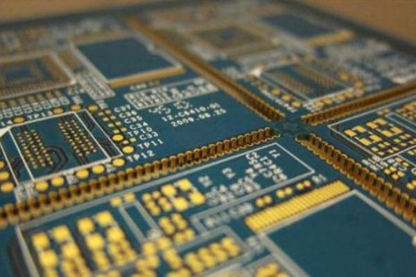
In Rigid PCBs:
The width and thickness of the traces have an impact on the impedance. Therefore, the width and thickness of the trace are chosen wisely to achieve the desired impedance. While manufacturing the PCB, the manufacturers check the width and thickness carefully and suggest changes if required.
Trace length is important as the impedance depends on it. The longer the trace, the more will be the resistance and inductance. Moreover, the trace length is also responsible for the delay of the signals. If you want two signals to reach at the same time, their traces must have the same length. Similarly, if there is a delay needed in any signal, the length of its trace is increased.
The dielectric constant matters a lot as it has an impact on the impedance of the circuit. The capacitance depends on the dielectric constant, and so does the reactance. Every material has a specific dielectric constant; thus, the material of the prepreg and core is selected according to the requirement.
The thickness of the core and prepreg also change the impedance of the PCB. The manufacturers keep an eye on the thickness of each layer to ensure the desired impedance.
The impedance falls when the copper thickness rises. Reducing the copper thickness and weight would enable a higher impedance.
In Flex Circuits:
- Hatch Width (HW) and Hatch Pitch (HP)
- Polyimide (PI) thickness of the FCCL
- Signal trace’s width/spacing and thickness
- The thickness of Adhesive in-tween FCCLs
- Dk (/Er) value of Polyimide (PI)
- Dk (/Er) value of Coverlay
- Dk (/Er) value of Adhesive
The PCB designer must therefore make sure that for high-frequency signals, their choice of trace and stackup makes it possible to achieve a target impedance value with a certain tolerance. The most advanced electronics CAD design tools calculate this automatically.
Things to Consider in Impedance Controlled PCB
- Differential Pairs
The differential pairs in the circuit can create issues, so their traces are created with more precautions. They are kept parallel and symmetrical to ensure distortion less transmission of the signal.
- Distinguishable Trace Width
The trace whose impedance is controlled must have a different width. There can be a slight difference in the trace to distinguish from other traces of PCB.
- Placement of Components and Vias
The vias and components are placed away from the differential pairs. The trace should not be disturbed by them, and they should be placed at suitable positions. The wrong placement of components and vias can create issues in the impedance, and consequently, the differential pairs are affected.
- Spacing Between Traces
The traces cannot be very close to each other. For differential pairs, the distance between the adjacent pairs should be at least five times the width of the trace. The distance between impedance-controlled traces and other traces should be 2-3 times the trace width.
Applications of Controlled Impedance
Controlled Impedance should be considered for PCBs used in fast digital applications such as:
- Telecommunications
- Computing 100MHz and above
- High-Quality Analog Video
- Signal Processing
- RF Communication
Impedance Control In PCB Design
Electrical Impedance: A measure of opposition to time-varying electric current in an electronic circuit.
The Problem: “A,” “B,” and “C” signals all reach the component at the same time.
The Solution: Apply Impedance to Circuit “C” to slow the signal enough for the component to first calculate (“A”+B”).
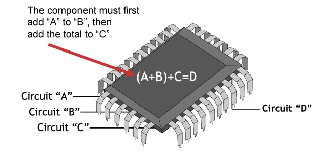
Similar to a cable, the signal encounters a change of impedance arising from a change in material or geometry. Part of the message will be reflected and partly transmitted. These reflections are likely to cause aberrations on the signal, which may degrade circuit performance (e.g., low gain, noise, and random errors). In practice, board designers will specify impedance values and tolerances for board traces and rely on the PCB Manufacturer to conform to the specification.
When rise times continue to reduce, inevitability, the number of traces requiring impedance control will continue to increase. Where impedance control is needed, it is essential to calculate it accurately with the most representative cross-section we can create.
Helpful Resource:
PCB Routing: How to Ensure PCB Impedance Control with Formulas and Resources
How to Calculate Impedance Control?
Determining impedances on a PCB is important and requires some particular measurement methods. Let’s take a look at some impedance control measures that are credible, accurate, and reliable.
- Smith Chart
The Smith chart was around before computers or PCB designing software was prevalent. The chart is used to describe the relationship between source and load impedance with the help of graphics. It also relies on an array of mathematical calculations to give an impedance value for a particular trace. - Computer Simulation
The software of today uses complex technology to determine control impedance numbers. The benefit of these programs is that they can merge your design considerations into a simulation to see a virtually finished product. However, this software is typically expensive to buy and use for modeling a finished PCB design. - Online Impedance Calculator
Online calculators are much more efficient and widespread than design software with PCB impedance control features. You can find out the controlled impedance for a trace through these calculators. These calculators are not as precise as the simulators, but you always get a ballpark figure to get the process rolling. Minor tweaking afterward can keep you safe because most of these calculators use standard numbers from the design guides for high-speed impedance boards.
All three methods listed above provide a good starting place for your calculations. No matter which method you adopt, you start with a safe set of rules compared to no impedance calculation.
How to do impedance control in PCB?
There are 5 methods that enable efficient impedance control in a PCB board:
- Give clear signals in PCB design
It is a good idea for the PCB designer to specify which signals require impedance control at design delivery.
A component data sheet is also included and provides information on each component’s signal class and corresponding impedance values.
Also, indicate which layer is more appropriate to pass individual signals and which spacing rules must be used between traces.
- Choose the appropriate transmission line form: microstrip line and stripline.
Microstrip lines are widely used for high-frequency transmissions, such as antennas, filters, and power dividers. A microstrip line for the outermost layer of a PCB is an electrical transmission line that can be fabricated using printed circuit board technology to transmit microwave frequency signals. Microstrip devices can be built on common FR-4 substrates to reduce costs in typical applications.
It consists of conductive strips separated from the ground plane by a dielectric layer called the substrate. The resistance capability depends on the dielectric constant, the insulating material’s thickness, and the traces’ width and thickness. These factors affect the impedance value, so the circuit’s operating frequency should also be selected in the design stage.
- Ensure that all the traces and components on the PCB have a certain distance
In PCB design, impedance-controlled traces should be appropriately spaced from other traces and components on the PCB to eliminate crosstalk as much as possible. This phenomenon generally affects microstrip lines. Therefore, we recommend that the minimum spacing should be “2W” (W represents the line width of impedance control), and “3W” is the best if conditions allow.
When it needs to be applied to the scene of transmitting high-frequency signals, the minimum distance should be increased to “5W”. Keep at least 30 mils away from any other type of trace for better isolation.
- Unify the length of the traces.
Unifying the length of the traces during signal transmission avoids the delay of the signal frequency (this is based on the fact that all traces are kept constant). It is essential in a high-speed propagation signal group to ensure that all signals can reach the destination simultaneously.
If the signal comes from a different point, a serpentine is usually inserted in the shorter trace to compensate for the length relative to the other traces.
- Control the use of capacitive components.
If you can try not to use components and capacitors between signal traces, any component will have some filtering interference in the impedance value. If the placement of capacitors is unavoidable, they should be placed symmetrically to achieve signal unity across all traces.
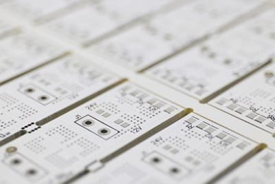
Impedance Control PCB Manufacturing
To meet the growing demand for impedance control PCB, PCB manufacturers have invested a lot of money and workforce and material resources in production technology to meet the production requirements of customers.
Due to the difficulty of impedance control PCB production, PCB manufacturers generally require PCB designers or purchasers to provide more detailed information and requirements, such as the type of material needed, copper weight and thickness of the board, the number of layers, Gerber file, so that the manufacturer can prepare the bill of materials (BOM). Impedance information should be marked in the Gerber file. If the necessary information is lacking, even a little critical information will make it difficult or impossible for the manufacturer’s engineers to know exactly what the customer needs.
Impedance-controlled PCBs are also divided into three different situations:
- No Impedance Control: This is a situation where you do not need any extra design elements to ensure correct impedance because you have very loose impedance tolerance. Naturally, this will result in a faster-completed, less expensive board because the manufacturer does not have to include any special measures.
- Impedance Watching: What is impedance watching? This is a situation where the designer will outline the impedance control trace, and the PCB provider adjusts the trace width and dielectric height accordingly. Once the manufacturer approves these specifications, they can begin to manufacture the board. You can request a Time Domain Reflectometry (TDR) test to confirm the impedance for a fee.
- Impedance Control: Actual impedance control is something you will typically only request when your design has tight impedance tolerances that could be tough to hit the first time around. When the capability limits of the manufacturer get close to the dimension requirements, it can be tough to ensure target impedance on the initial attempt.
In the case of impedance control, the manufacturer makes the circuit board achieve the target impedance as far as possible. Then they tested TDR to see if they succeeded. If not, they adjust accordingly and try again until they reach the required impedance.
Helpful Resource:
Impedance Control: How to Specify Your Requirements for PCB Manufacturers
Impedance Control PCB Fabricator
JHYPCB is a leading manufacturer in Asia and can provide services in most of the countries of the seven continents. Our large facility has 500+ experienced employees to ensure fast turnaround and high-performing PCBs. We can deal with all types of PCBs and PCBAs and offer prototype and turnkey assembly services. Our facility can handle small to large volume orders and ensure the quickest delivery at cheap rates. We are ISO, RoHS, and UL certified.
We offer high-quality Impedance Controlled PCBs at cheap rates. The buyer can even order one PCB or PCBA to check their designs. Your order will reach your doorstep without any hassle. For more information, quotes, and queries, feel free to contact us.
FAQ
Controlled impedance is the characteristic impedance of a transmission line formed by PCB conductors. It is relevant when high-frequency signals propagate on the PCB transmission lines. Controlled impedance is important for signal integrity: it is the propagation of signals without distortion.
Impedance matching. Impedance matching means that when energy is transmitted, the load impedance must be equal to the characteristic impedance of the transmission line. In high-speed PCB design, the matching of impedance is related to the quality of the signal.
The characteristic impedance of a PCB trace is typically determined by its inductive and capacitive reactance, resistance, and conductance. These factors are a function of the physical dimensions of the trace, the dielectric constant of the PCB substrate material, and dielectric thickness.
Impedance intuition is readily acquired through two simple equations. Trace impedance “Z” is directly related to trace inductance (L) and capacitance (C), or Z=sqrt(L/C).
At the compromise value of 50 ohms, the power has improved a little. So 50 ohm cables are intended to be used to carry power and voltage, like the output of a transmitter.
Why is impedance important? It is used for determining the interrupting capacity of a circuit breaker or fuse employed to protect the primary of a transformer.
Antenna impedance relates the voltage to the current at the input to the antenna. Let’s say an antenna has an impedance of 50 ohms. This means that if a sinusoidal voltage is applied at the antenna terminals with an amplitude of 1 Volt, then the current will have an amplitude of 1/50 = 0.02 Amps.
In electronics, a signal trace on a printed circuit board (PCB) is the equivalent of a wire for conducting signals. Each trace consists of a flat, narrow part of the copper foil that remains after etching.
Recommended PCB Manufacturing Services


Advanced Learning
- Five factors that FPC PCB designers should know about impedance control
- What are the aspects of PCB Design For Manufacturing (DFM) and Design For Assembly (DFA)?
- Find Out Now, What Should You Do For Fast PCB Classification?
- IPC Standards: A Guide to Standards for PCB Manufacturing and Assembly
- How to Choose the Right PCB Manufacturer and Supplier