
Through-hole PCB Assembly Service
Perfect Application of PCB Through-hole and DIP Assembly Technology.
We provide through-hole PCB assembly services to meet the conventional lead assembly requirements of various industries. We provide single-, double-sided, and high-density multilayer PCB through-hole circuit board assembly services to meet our clients’ low to mid-volume production requirements.
Home » PCB Assembly » Through-hole PCB Assembly
There are two main assembly methods for components on a printed circuit board (PCB): Through-hole Assembly and Surface Mount Technology.
Get one-stop through-hole PCB assembly (THA) from prototypes to mass production. At JHY, we are committed to delivering high-end printed circuit board assembly technology solutions. To this end, we offer a complete range of through-hole PCB assembly and surface mount technology capabilities resulting in PCBAs that comply with the highest industry quality standards.
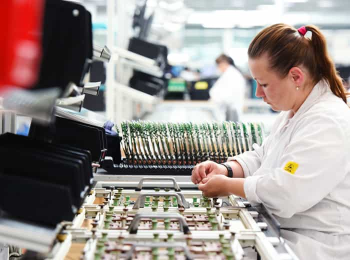
Our through-hole PCB Assembly services comprise both manual and automated techniques. While our manual techniques can handle complex assemblies, automated ones are best suited for low-volume production. We offer thru-hole assembly at the highest quality level and cost-effectively.
Introduction to Through Hole Technology (THT)
Through-hole PCB Assembly
What is Through-hole Technology?
Through-hole technology or Through-hole Assembly is the mounting process by which component leads are placed into the drilled holes of a bare PCB and soldered to the pads on the opposite side. This can be done using manual assembly or automated insertion mount machines.
- THT is still one of the important mounting processes
- Manual and automated insertion of Components
- Popular in the 1950s and is an ancient installation technique
- Use wave soldering or selective soldering techniques
- Apply in military or aerospace equipment or where high-Tg are present
- Radial or Axial Leads Components.
- The components can be mounted vertically or horizontally.
THROUGH HOLE Technology
Why Through-hole PCB Assembly?
The mechanical strength of PCB through-hole connections is higher than most surface mount connections. In contrast, the bonding strength of PCB surface mount components does not exceed the multilayer PCB board surface’s bonding strength. With the miniaturization of devices, the amount of solder decreases, and the connection strength also decreases.
Through-hole PCB technology process fixing components are most suitable for high-reliability products that require high-strength connections between multilayer boards. The surface mount device (SMD) is only set on the circuit board’s surface with solder, and the lead of the through-hole fixing component runs through the entire circuit board, and the part can withstand more significant environmental stress. Too much solder and it could get into other connections and cause a short. Too little and you may not have a strong enough joint. Cold solder joints could break, and if you get the connection too hot you may cause some damage to the components or the board.
Therefore, through-hole PCB assembly technology is usually used for military, automotive, and aerospace products that may have extreme acceleration, collisions, or high temperatures. Through-hole assembly technology is also suitable for testing and prototyping applications that sometimes require manual adjustment and replacement of devices.
Thru Hole Assembly Advantages
Benefits of Through Hole PCB Assembly
There are many benefits and advantages to through-hole PCB assembly, including:
- Compression resistance: Compared to surface mount components, through-hole parts can withstand higher mechanical and environmental stress levels. Therefore, through-hole components are more suitable for large components that must withstand high power and high voltage.
- High heat tolerance: through-hole components are known for their high heat resistance and can be used in military and aerospace equipment applications.
- High reliability: Through-hole PCBs are best used for high-reliability products that require stronger connections between layers.
- Ease of Prototyping: Through-hole PCBs also lend themselves to ease of prototyping and improved reliability, and Through-hole components are easier to replace or adjust their position.
- Strength of Bonds: Through-hole assembly involves sticking required components through a circuit board and then attaching them with a metal solder, strengthening the connection between the circuit and its components.
- Durability: Stronger bonds between the circuit and its components indicate better durability and the capacity to handle harsher conditions without substantial wear and tear or damage.
Little surprise, though surface mount components allow for denser configurations, for larger and heavier components that require strong bonds, through-hole technology has remained resilient and relevant.
One-Stop Services – PCB Assembly & Testing

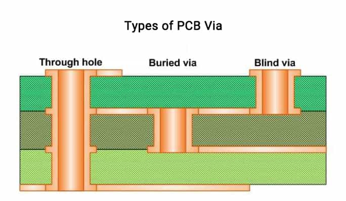
PCB Via Size Guidelines For Manufacturing
Vias are the “tunnels” on PCBs. You may be surprised to find out that your PCB contract manufacturer will typically think of a via as any hole in the board. Whether a hole is serving as a net interconnect or being used for soldering the lead of a thru-hole component, it is still a via to your PCB manufacturer. If vias aren’t planned out correctly, they can cause problems during the manufacturing of your board. Let’s look at some of the common issues that can happen during PCB manufacturing with Vias and how you and your contract manufacturer can avoid these problems by following good PCB via size guidelines.
How PCB Manufacturer Categories PCB Vias
For PCB fabrication, any hole in a printed circuit board can be considered via. This includes non-plated through-holes and plated through-holes for parts, as well as an assortment of interconnect vias. These interconnect vias include through-hole, blind vias, buried vias, and micro-vias.
A through-hole via a surface mount pad is often considered a different type of via because it usually requires unique design rules within the CAD tools for use. For fabrication purposes, however, these are still considered a regular thru-hole filled via.
As far as PCB assembly goes, the major via consideration are those thru-holes that will be used for installing parts. These include regular thru-hole components that will be soldered into plated thru-holes, such as connectors, resistors, and capacitors. Also in this category are parts that are installed into holes that are not soldered. These would include connector legs, press-fit parts, guide pins, screws, and other mounting hardware.
Problems With Vias That Can Affect Assembly
When via holes for thru-hole components aren’t fabricated correctly, there can be a lot of problems during assembly:
- Holes that are too small for the component lead intended for that via could cause bent leads or the inability to install the component. A part that can’t be installed can ruin an assembly, while bent leads may cause soldering problems and intermittent electrical problems. All of this may result in the PCB having to be refabricated.
- The plating process on smaller holes can be more challenging to work with, leading to inconsistent hole sizes. Once again, you may run into component insertion or solderability problems. It is much easier to maintain consistent plating on larger holes.
- Larger holes also can cause problems, such as loose parts that require care in soldering, but these problems are usually easier to fix and can often be resolved with manual assembly processes.
- Larger vias used on large ground pads under surface mount components, such as BGAs, may cause the solder to wick through and compromise the connection. This can impact the part’s electrical, mechanical, and thermal characteristics, resulting in its failure.
- Large plated thru-holes used for grounding hardware, such as screws or posts, must have enough clearance on all layers to accommodate the larger drill tolerances; otherwise, these holes may end up shorting to other layers if the drills exceed the expected tolerance.
It is also essential that holes of the same size with the more extreme precision and registration be specified as the “first” to be drilled. Those same sized holes with greater tolerances should be defined as “seconds” to be drilled. If this sequence isn’t correct, the holes with the tighter tolerances may end up being drilled after the drill bit has been worn down, resulting in miss-drilled holes. Ensuring the correct drill tolerances for priority drill sequencing can help you avoid these problems and ensure a successful assembly.
PCB Via Size Guidelines to Avoid Assembly Problems
Some via hole size considerations to remember when setting up the vias in your PCB design include:
- Smaller vias: These vias are essential in supporting smaller-pitch/higher-density components, such as 0.5mm BGAs, but they are more sensitive to drill and plating errors, which can cause PCB failures. Only use these smaller sizes when necessary. It is much better for manufacturing to use an 8 mil hole instead of a 5 mil hole if it will only take minor layout modifications.
- Larger vias: These are much easier for the fabricator to work with, but the correct tolerances and clearances must be used to ensure there aren’t any shorts to other layers. It is also essential to consider where larger vias will be so that they don’t pull the solder away from ground pads that need a good connection to their component.
- Blind and buried vias: These are essential for high-density, high-speed, noise-sensitive designs, but their advantage comes with a price. These vias require increased fabrication costs and time to process the vias first before laminating the board’s layers together.
- Too many vias of the same size: Try to vary the drill sizes so that you don’t have too many holes that are the same size. For those boards with a high density of the same drill size, the drill bit may not be able to keep its integrity for the entire drill operation. This requires the fabricator to stop the drilling process partway through, replace the drill bit, re-register the board, and then continue the operation.
- Plating: Your holes will be plated with copper for connectivity unless you specify the hole as unplated. Ensure that you select the correct size for the drill needed for the hole taking into account the plating. Usually, this is done by specifying the “finished” hole size. If the finished (plated) hole size isn’t accounted for, you may end up not being able to insert the component leads into their holes.
Not only will keeping these via considerations in mind help you to create a better design, but these are also part of the list of design issues that a quality PCB manufacturers will have their engineering staff looking for. By including the best via design practices initially in your PCB, there will be less design cleanup needed to get your board through the assembly.
What can we do for you?
The drilling of your printed circuit board will take place at the fabricator. They must do an excellent job of eliminating any potential assembly problems due to size. The more complex or stringent the via requirements are in your design, the more specialized the fabrication vendor needs to be. To ensure your PCB is fabricated correctly, you need a contract manufacturer that fully understands the process and has substantial business relationships with multiple fabricators. This way, they can choose the best fit for the board technology that you are having built.
This all starts with working with your PCB contract manufacturer that understands the specific requirements of your design. That is why at JHYPCB, we take the time to give your system a full review beforehand to know upfront what you will need. This enables us to choose from the list of our fabrication vendors that we have been cultivating over many years, the best possible fit for your board. This way, when we get your commission back in-house, there won’t be any problems with assembly due to via size problems.
Through-Hole PCB Assembly Highlights
Our through-hole PCB services have gained popularity due to the accuracy of PCBs that we provide. This quality comes from our experience, expertise, and automated equipment to perform various through-hole PCB assembly processes.
- We have automated insertion equipment for placing components axially or radially. We use various such equipment for high-speed installation of through-hole components.
- Reflow oven in our facility allows us to fix soldering paste appropriately.
- Automated wave soldering system allows us to precisely solder through-hole components.
- Advanced aqueous washing system for removing contaminants from the circuit boards.
- We use computer-controlled selective soldering machines for reducing errors that may occur during tin-lead or RoHS Through-hole assembly. This helps us reduce errors, as well as the costs of manufacturing.
- We provide in-house conformal coating, as well as device programming.
- All PCBs are built to ANSI/J-STD-001 and IPC-A-610-D standards.
Advanced Learning: IPC Standards: A Guide to Standards for PCB Manufacturing and Assembly
Through-hole PCB Assembly Service Capabilities
Our strong PCB assembly capabilities can fully handle through-hole PCB assembly services, including Manual and automated placement of components, RoHS soldering using tin-lead solder, selective soldering, functional testing, etc. Best of all, we have a team of experienced and well-trained assembly workers who are good at hand soldering through-hole components, automatic insertion of axial and radial components, and more. In addition to through-hole PCB assembly, we also provide value-added services such as conformal coating, IC programming, surface finish, and more. The following capabilities allow us to take up any regular and complex PCB assembly project.
Components | Connectors and terminals BGA, uBGA, QFN, and Leadless chips Fine pitch to 8 Mils |
Board Type | |
Board Shape | Slots and Cut outs Rectangular Complex and Irregular Round |
Component Package | Loose parts and bulk Reels Tube and tray Cut tape |
Assembly Process | Leaded process Lead-Free (RoHS) |
Board Dimensions | Largest size: 15″ x 20″ Smallest size: 0.2″ x 0.2″ |
Design File Format | Centroid(Pick-N-Place/XY file) BOM (Bill of Materials) (.xls, .csv, . xlsx) Gerber RS-274X |
Our Through-hole PCB Assembly Testing and Inspection Capabilities
The following testing capabilities make us one of the best in the industry:
- In-Circuit Testing: This type of testing is conducted for high volume production lines and helps us check every minute soldering and other components in detail.
- Automated Optical Inspection: Abbreviated as AOI, these tests are performed to ensure that product is free from soldering, component, and BGA defects.
- Automated X-Ray Inspection (AXI): This testing is performed to inspect short fills, short circuits, fills, etc. The mechanical X-ray inspection helps reduce the number of defects and improve the quality of the Through-Hole circuit.
- Burn-in Tests: These tests are performed on components to detect their failure or reliability in real environments.
- Assisted Visual Inspection: Our experts use a wide range of advanced visual inspection equipment to perform a detailed inspection of soldering and component placement accuracy.
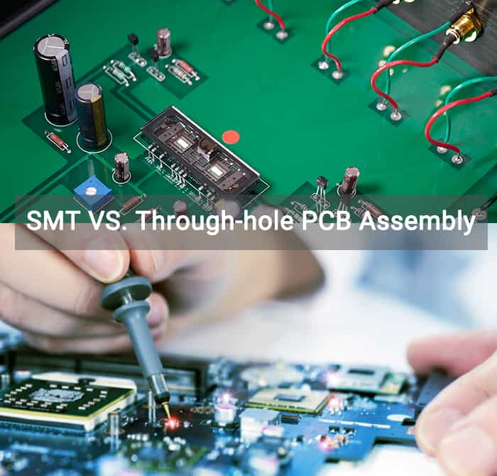
SMT vs. Through Hole Parts: Why the Difference?
When printed circuit boards first became a staple in electronics production, through-hole parts were the only available components. As time went on, however, SMT parts slowly became more prevalent until they eventually became the dominant component package style used on PCBs today. There are several reasons for the popularity of SMT parts now, including:
Size: Without the need to lead to poking down through a drilled hole, an SMT part is, by default, a smaller part. This makes it much more attractive to designers trying to fit more circuitry onto smaller board sizes in today’s electronics.
Expense: Since an SMT part is, by default, a smaller amount, it is also less expensive to manufacture. This makes SMT parts more cost-effective than their through hole counterparts.
Availability: With SMT parts being smaller and less expensive, they have mostly replaced theirs through hole counterparts. This is especially true with passive parts like resistors and capacitors, where the SMT component package is often the only option anymore.
Electrical Performance: Smaller parts have less distance for electrical signals to travel through, which lowers the signal’s flight time. This makes SMT components the better performers electrically than their through hole counterparts.
For these reasons, it would be tempting to think that all PCB components should be surface mount parts. There are, however, some excellent reasons why through hole parts are still used in the assembly of circuit boards:
Power: For components used in high power circuits, SMT packages are not a good option. High power parts often have more metal in them, making it more difficult for surface mount soldering techniques to achieve a good solder joint. Additionally, the larger sizes of power parts often require the more robust mechanical connection of a through hole for high voltages, thermal and mechanical stability.
Strength: Components such as connectors, switches, or other interface parts need the force provided from the leads being soldered into a drilled hole. The constant physical stress that the parts go through from regular use could eventually break an SMT solder joint.
Availability: Some components, especially those larger parts used in high power applications, aren’t available yet in a real SMT equivalent.
These are the significant reasons why components are divided between SMT and through hole packages. These two packages also affect how a printed circuit board is manufactured.
SMT vs. Through Hole for PCBAs: Wave Solder and Solder Reflow
Two different ways printed circuit boards have their components soldered onto them: wave solder and solder reflow. Although there can be exceptions, through hole components are usually wave soldered, and SMT components are usually solder reflowed. After the through hole components are inserted into their drilled holes, the circuit board is run through a molten wave of solder that wicks up into the hole around the lead and forms a solid solder joint.
For SMT parts, solder paste is applied to the parts’ pads allowing the leads of the component to be held in place. The circuit board is then run through an oven, which causes the solder paste to reflow and forms a solid solder joint between the leads and the pads. For circuit boards with both through hole and SMT on them, a mixture of the two methods is required. In some cases, portions of the board are masked off to go through the wave solder, while in other instances, the through hole parts may be manually soldered.
The SMT assembly line is typically both faster and less expensive. The automated pick and place machines can reliably handle various components during one run, while the through hole parts are often manually inserted by hand. The reflow ovens reflow the solder paste that has already been applied to the SMT pads, while the through hole parts have to be run over a wave of solder. This wave has to be continually supplied from a temperature-regulated source of molten solder, which is a more costly process than the SMT parts going through solder reflow.
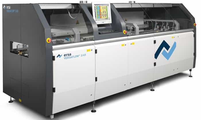
Selective Wave Soldering Machine for Through-hole PCB Assembly
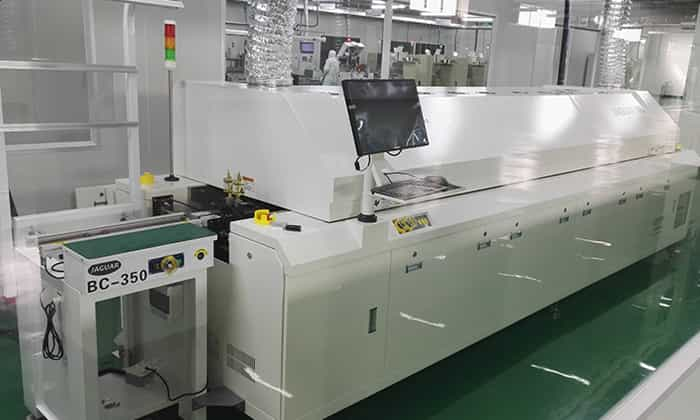
Reflow Soldering Machine for SMT PCB Assembly
SMT vs. Through Hole for PCBAs: How to Choose?
Based on the manufacturing process, it would be easy to say that SMT components are the best choice to use on your printed circuit board design. But that isn’t the case. The truth is that both of these component package styles are important. Although most passive and integrated circuits will come in an SMT package, it is still essential to use standard through hole parts for your connectors, switches, and other mechanical or power parts.
Additionally, legacy boards are still being produced that have to have older through hole parts used to satisfy the copy exactly requirements.
Although SMT components are less expensive, smaller, and better performers, the world of circuit board design and manufacturing has not seen the end of through hole components. These vital parts are going to be with us for a long time, and for excellent reasons. The critical factor for you is to choose the right amount for your specific application. Your next choice is just as important: you need to use a PCBA manufacturer that has the experience and facilities to manufacture both types of component packages expertly. You need to know that all of your board’s components are soldered into place with good concrete solder joints to ensure the most significant level of quality for your board.
Through Hole Technology Process
No matter which process is used, through-hole technology or surface mount technology, both of them must meet the soldering standards. The processes of them are the same:
- Manufacture the required PCB board (Single or Panel)
- Pick-and-Place (Automatic or Manual)
- Soldering (Reflow, Wave Soldering, or Selective Soldering)
- Inspection (X-ray, AOI, Manual Visual)
- Cleaning (Ultrasonic/Water-based Cleaning)
- Breakaway (For Panel)
- Testing (ICT, FCT…)
The difference is mainly in the placement of components and soldering.
Adhering to IPC Through Hole Soldering Standards
There is a reason why your PCB contract manufacturer is the go-to expert when making your printed circuit board, and that is because they should have the skills, experience, and industry standards from which to work. Here, we’re going to take a look at the IPC through-hole soldering standards and how a high-quality contract manufacturer will apply them to working on your printed circuit board assembly.
What IPC Through Hole Soldering Standards Apply to PCB Manufacturing?
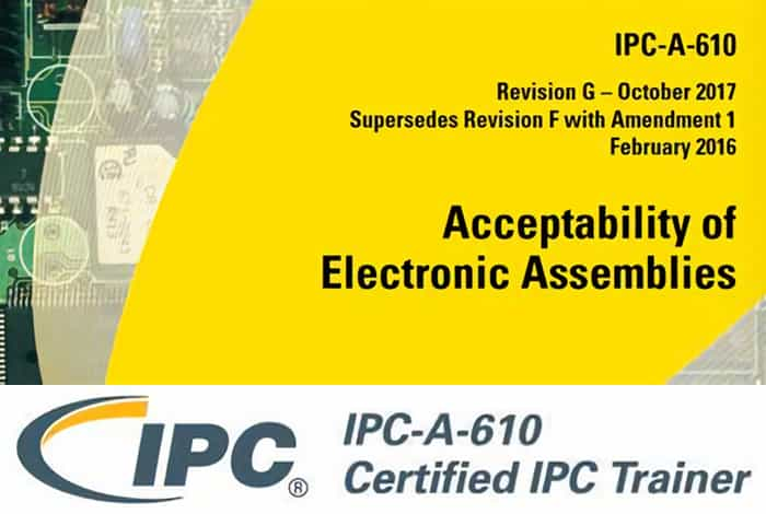
For soldering through-hole components onto circuit boards, IPC-A-610G—the Acceptability of Electronic Assemblies, is the applicable standard. This standard covers many aspects of printed circuit board assemblies, including definitions of PCB terminology, installing components on a PCB, and of course, soldering various parts onto the board. Contract manufacturers should use this standard as their guide when developing and maintaining their own specific through-hole soldering processes and procedures.
Section seven of this standard covers through hole component technology and the requirements for successfully soldering these parts onto a PCB. The main concern for PCB contract manufacturers when building boards is the proper formation of a good solder joint. The IPC-A-610 standard specifies how to achieve a good solder joint with requirements for the solder’s adequate wetting, combined with the amount of solder fill necessary for a plated through-hole.
From here, the contract manufacturer should develop their assembly processes to satisfy these requirements. These processes include:
- Component preparation for assembly.
- Component loading into automated assembly equipment.
- Wave solder.
- Selective solder.
- Manual solder (hand soldering).
- Touch-up soldering.
Each of these processes is specifically designed to meet and exceed the requirements for through hole soldering as specified in the IPC-A-610 standard.
Through Hole Soldering Standards for PCB Rework
Once a printed circuit board has come through the automated soldering processes, there still may need to be manual soldering done to the board. This manual work may be part of the initial manufacturing process, or it may be reworked to correct any assembly problems or make changes to an assembled board. Once again, there is a standard that covers how this work should be done.
IPC-7711C/7721C shows the step-by-step process of modifying or repairing circuit boards. The standard contains illustrated chapters for most every PCB repair imaginable and also covers the equipment required for the repairs. Here are the basics the standard covers for through hole soldering modifications or repairs:
- Identifying, removing, and eventually replacing conformal coating on the PCB to facilitate the rework.
- Unsoldering through hole components for removal using vacuum or wicking.
- Repairing a damaged plated through hole.
- Reinstalling and soldering through hole components.
- Changing or correcting silkscreen associated with modified components.
In addition, the standard covers many other aspects of PCB rework and repair. These include:
- Delamination or blister repair.
- Bow and twist repair.
- Hole repair by either patching it with epoxy, or removal and replacement of metal barrel.
- Base PCB material repair.
- Broken or lifted conductor (traces) repair with sealers, adhesives, foil jumpers, or wires.
Both of these standards cover a lot of detailed information that your PCB contract manufacturer should put to use when building your printed circuit board assembly.
Soldering Expertise at Your PCB Contract Manufacturer
Knowing and applying these standards on through hole soldering is the key to success when assembling printed circuit boards. The best PCB manufacturers will embrace the entire standard rather than just focusing on the specific details needed to build an acceptable PCBA. This way, they will already have the infrastructure in place to ensure the best possible conditions for building a printed circuit board. With proper PCBA handling, lighting, equipment, procedures, and other work environment and personnel considerations, following the requirements of the standard will end up being a natural part of their regular workflow.
At JHYPCB, we have that infrastructure already in place. Our facilities are modern and specifically designed for high-quality PCBA manufacturing, and we have more than 10 years of experience building many different types of boards. We meticulously maintain our soldering equipment, from the smallest soldering iron tips to our large wave solder machines, and use the best solder, fluxes, and other materials to ensure the highest quality on the boards we build. Additionally, we employ certified IPC trainers (CITs), giving us the ability to keep our own staff at their peak efficiency, as well as helping our customers and suppliers to understand our manufacturing processes.
One-stop Turnkey PCB Assembly Manufacturer
We can provide PCB prototypes to high volume assembly services at shorter turnaround times. Our through hole printed circuit board services are designed to provide high-quality products to mission-critical applications to industries such as aerospace, electronics, instrumentation, and military. To know more about Through-hole assembly services, and other PCB assembly services, you can call us at +86 13825274100, or email at sales@pcbjhy.com. We will get back to you within one business day.
Through Hole PCB Assembly FAQs
In the Through-hole technology, the leads of the components are inserted into the via holes drilled in bare circuit boards and soldered to pads on the opposite side either by automated assembly insertion or manual assembly.
The through-hole technology mounting components are called axial and radial leads components.
Through-hole PCBs find extensive use in:
- Medical devices
- LEDs
- Consumer electronics
- Industrial equipment
- Automotive components
- Aerospace components
- Telecommunication equipment
- Defense and military applications
Whether to choose Through-hole technology Or surface mount technology depends on your design and the project’s requirement. Most of the integrated circuits go for the SMT package. However, the standard way for connectors, switches, or mechanical power parts is to use through-hole components.
Yes. To ensure the quality of through-hole PCB assembly, we inspect the boards using X-Rays and offer total reliability.
Yes, based on your requirements, we are well-equipped to offer first-article inspection service for through-hole PCB assembly.
Our turnaround times depend on your requirements, we offer standard turnaround times and quick turn through-hole PCB assembly services.
The through-hole PCB assembly cost is based on some factors, including the types of through-hole PCB components, order quantity, and more. Once you reach out to us with your custom requirements, we will revert with a custom quote for through-hole PCB assembly.
Advanced Learning
- PCB Assembly Capability
- LED PCB Assembly
- Fast Prototype PCB Assembly Service
- PCB SMT Solder Paste Stencils
- Components Purchasing Services
- What is the Bill of Materials(BOM), and how to create one?
- PCB and PCBA Manufacturing Files
- How to Store PCB and PCBA?
- How long can PCBA finished products be stored?
- How to Use PCB Stencil-Step by Step Guideline
- Shenzhen – The Global Hub for High-Quality PCB Assembly Manufacturing
- Evaluating and Selecting Quick-Turn PCB Assembly Manufacturers in China
- Leveraging Turnkey PCB Assembly Manufacturing Services
- Choosing the Right PCB Assembly Manufacturer for Your Needs