With the development of electronic products’ PCBA assembly towards miniaturization and high assembly density, SMT Surface Mount Technology has become the mainstream electronic assembly technology. However, due to the excessive size of some electronic components in PCB assembly and processing, plug-in processing has not been replaced. Still, it plays a vital role in electronic assembly and processing. Therefore, there will be a certain number of through-hole components in the PCB. The assembly of both plug-in parts and surface assembly components is called a mixed technology PCB assembly, short for mixed assembly. The assembly of all surface assembly components is called full surface mount. PCBA assembly method and its process flow mainly depend on the type of components assembled and the equipment conditions assembled.
PCB Assembly Manufacturing Steps
Step1: Procurement of Components/Material
First, the components and materials are procured according to the requirement of the PCB and the Bill of Materials (BOM) provided by the buyer. The components are bought, and if anything is not available, it’s replaced by a similar component after the permission granted by the buyer.
Moreover, Design for Manufacturability (DFM) is important. The experts check every document to ensure the smooth assembling of the PCB without any delays. It’s better to find the problems initially because it detects the errors and problems in the first step. It’s a good engineering practice, which is offered at JHYPCB.
Step2: PCB Fabrication
The next step is the fabrication of the PCB. PCB is fabricated according to the requirements of the buyer. After this step, there is a bare board without any components.
Step3: Application of Solder Paste
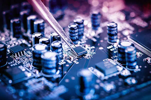
The next step in the PCB Assembly is the application of solder paste. A solder paste is applied to some regions of the PCB using a stencil. The paste is applied to the surface where the components will be placed in the future. This step is carried out through a machine.
The PCB is placed inside the machine, and the paste is applied over it. It’s similar to a t-shirt printing machine that prints using a stencil. The same is the case in the PCB assembly; the only difference is the solder paste instead of paint.
The stencil is placed over the PCB, and a roller is moved over it, which applies the solder paste to the PCB. The paste gets into the pads and holes of the board. The stencil is important to use; it’s a metallic stencil, which helps apply the solder to the required areas only.
Step4: Pick and Place
After applying the solder paste, it’s time to place the components on the board. It can be done manually, but for speed and achieving more accuracy, machines are used. The machine is fed with the reels of components. Different reels are placed according to the requirement. The machine picks the components and places them in the correct places. Therefore, this process is commonly known as Pick and Place. It’s an automated process in which the information is transferred to the machine from the files, and the machine does the work accordingly.
Step5: Reflow Soldering
Once the components are placed in the right place, it’s time to solder the components. As we have already applied the solder paste, we only need to melt the solder paste again so that the components can make proper electrical connections. For this purpose, the PCB is passed through a reflow oven. It’s placed on a conveyor belt and passes through the oven. This process is known as reflow soldering. The oven is hot enough to melt the solder, which holds the components and completes the electrical connections.
The board in the oven is very hot; therefore, it’s cooled before it comes out of it. After reflow soldering, the components are in their original places. The board is almost ready to use, but it needs to go through testing to ensure quality.
Advanced Learning
What is the difference between wave soldering and reflow soldering?
Step6: Inspection
Inspection is an important step that can pick the errors and flaws. Every PCB needs to go through this process to make sure it’s up to the mark. There can be a short circuit, wrong placement of components, or any other problem with the assembled PCB. Therefore, inspection is a critical step.
Inspection can be done manually and with the help of machines. Usually, the manufacturers manually check the assembled PCB to detect any visible fault, and then they go for other techniques that include X-ray and AOI. Manual checks are not reliable but are still used to detect faults in the PCB.
X-ray inspection is a powerful method that can detect faults in multilayer PCBs. The rays are passed through the layers and make everything visible. It’s an advanced method that is preferred for complicated PCB designs. But it can identify the problems with the PCB without any hassle. After an X-ray inspection, it’s easy to detect the fault and its root cause. Often the connections are under the components, and they are not visible to the naked eye and during AOI testing. Therefore, X-ray testing is used in such cases. It’s more reliable in assuring the quality of the PCB.
In this method, the rays are passed from the PCB, and they can even pass from the components. They can reveal the joints and electrical connections under the component. The rays are reflected and create an image, which can be analyzed using image processing. The image indicates the soldering joints and even their densities.
- AOI
AOI stands for Automatic Optical Inspection. This method is quicker and simpler than X-ray inspection, but it has limited use because it cannot see the connections under the components. It uses cameras to analyze the PCBA from different angles. It is fast, so it can be used to inspect a large batch of PCBs in less time.
Step7: Final Test
After inspection, final testing is done. The assembled PCB is checked whether it’s providing the desired results or not. It is tested using various methods. It is checked whether it’s providing the desired results or not. After final testing, the PCBA is shipped to the customer.
This is the last step of the PCB Assembly.
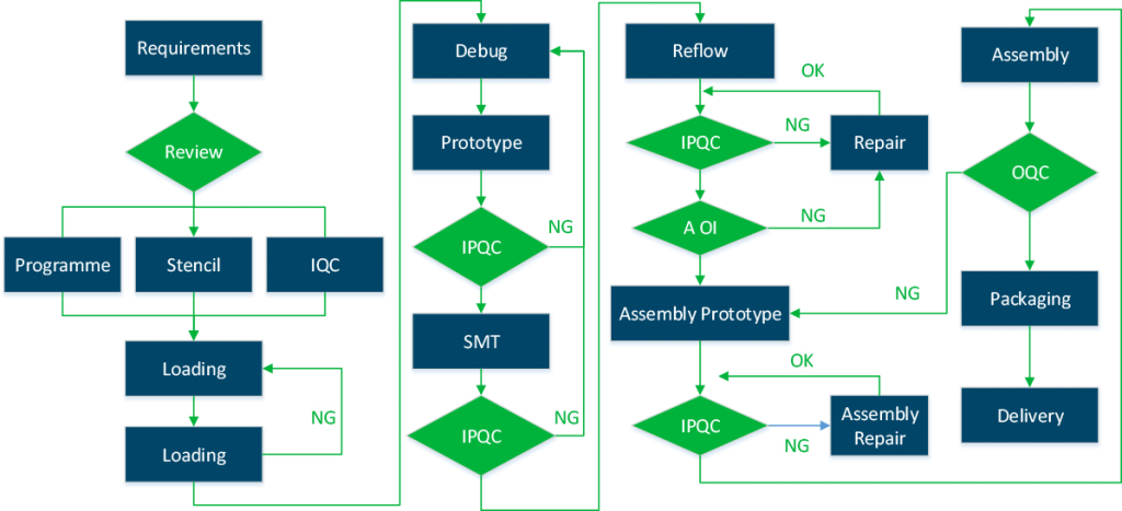
Electronic PCB Assembly Process Flow Chart
Related Posts
- How to Select the Right Low-volume PCB Assembly Manufacturer?
- The Advantages and Disadvantages of Surface Mount Technology (SMT)
- How to clean the PCB assembled boards? [Solved]
- Selective Wave Soldering Guidelines
- SMT PCB Assembly Manufacturing Process Introduces
- The Two Typical SMT Reflow Soldering Temperature Curve Modes
- 30 Common SMT PCB Assembly Defects
- Solder Paste and Solder Paste Printing in SMT PCB Assembly
- IPC Standards: A Guide to Standards for PCB Manufacturing and Assembly
- What is the Bill of Materials(BOM) and how to create one?


