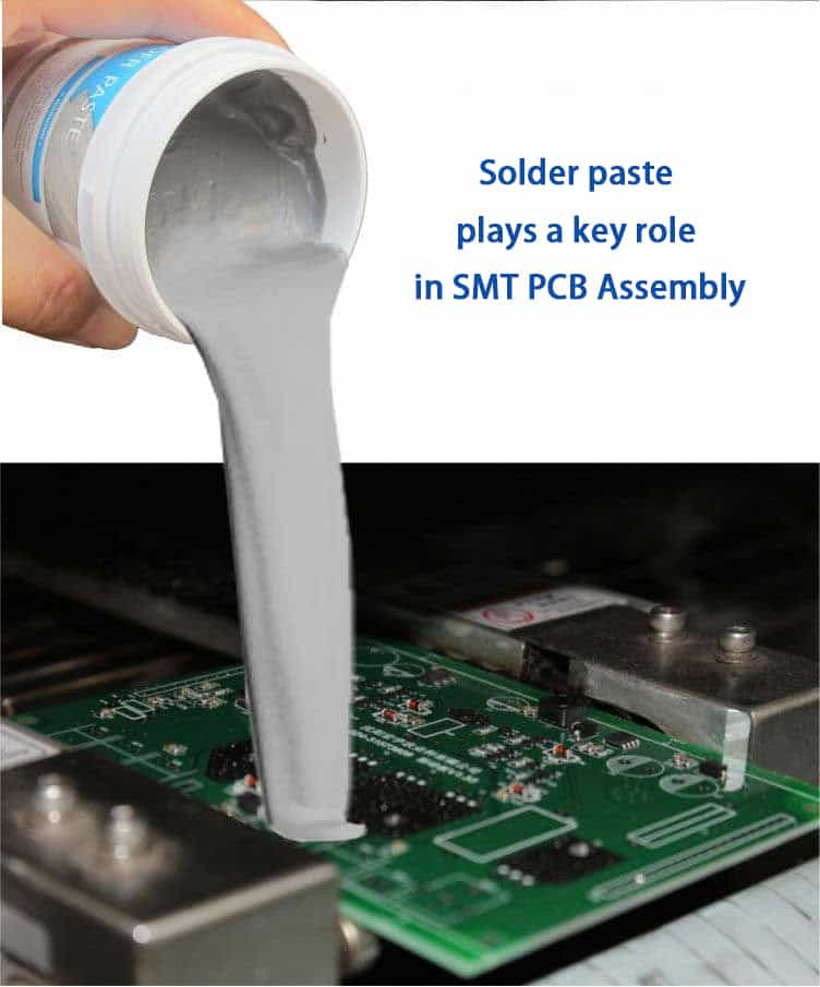
What is solder paste used for?
Solder paste plays an essential role in SMT, and it is widely used in PCBA. However, only a few people have an excellent command of solder paste, while most people know less about it.
Here is some basic knowledge about solder paste in SMT PCB assembly:
What is solder paste in SMT PCB assembly?
Solder paste is a new welding material that comes into being because of surface mount technology. And solder paste is so complex, a mixture of solder powder, flux, and other additives. Solder paste has specific viscosity at ordinary temperature and can mount the electronic components on initial positions. At the soldering temperature, the printed circuit pad and components will be permanently connected with the volatilization of solvent and some additives. It offers a solder medium to form solder joints in the reflow process with enough electrical and mechanical strength.
- Solder paste is a mixture of minute solder spheres held within a specialized form of solder flux.
- Solder paste is applied to surface mount boards before pick and place and, when passed through an infra-red reflow machine, melts to provide the soldered joints.
- Solder paste is the form of solder used in association with infrared reflow machines during the PCB assembly process.
- Solder paste is used in PCB assembly as it provides significant advantages, and its form enables the process to become a simple and easy process.
- The solder paste can be sued within large-scale PCB assembly or even within prototype production. It is used in most SMT assembly forms, proving easy to use the medium for the solder.
- Solder paste is a paste that can be easily applied to the PCB circuit board during PCB assembly.
- The solder particles are a mixture of solder. Traditionally this used to be tin and lead, but with the legislation introduced worldwide, only to use lead-free solders. These may be made from a variety of mixtures. One is 99.7% tin and 0.3% copper, whereas other mixes include other metals, including tin.
The main components of the solder paste
Flux
The main elements of instability as follow:
1). Activation:
Activation plays a role in getting rid of the oxide on the pad surface and components soldering part. Besides, it can reduce surface tension.
2). Thixotropic
It can adjust the viscosity and printing performance, which plays a role in avoiding the trailing and adhesion in solder paste printing.
3). Resin
Resin can enhance the adhesion of solder paste to protect and avoid re-oxide of PCB after soldering. It is essential in component mounting.
4). Solvent
The solvent can help dissolve the different chemical substances mixed in the flux and make flux coating smoother, promoting the flux effect. Also, it makes it easier to control the paste viscosity and fluidity.
Solder Powder
Solder powder is usually mixed with Sn, Ag, Cu, and Bi. The smaller size of solder powder can achieve a better result than solder powder that can be completely attached to the surface. However, on the other hand, the smaller size of solder powder means the higher probability to be oxide.
The classification of Solder – How many types of solder paste
Solder is a kind of fusible metal with a lower melting point than the metal being soldered and also has specific compression capabilities with good conductivity and fast crystallization rate. When the solder melts, it can wet the metal’s surface being soldered and form the alloy layer to connect the metal. It is widely used in electronic product mounting.
Solder has various categories. According to the melting point, solder can be divided into soft solder and hard solder. And the differences in composition make solder have several solder types: tin-lead solder, silver solder, copper solder, and so on. But in solder paste printing, PCB manufacturers usually use the tin-lead solder.
Tin-lead solder is the most popular in solder paste printing, and it is mainly composed of tin and lead, with some trace metal elements like Sb. Tin-lead solder is widely used in radiators and soldering of the electronic industry, and waving soldering dip and soldering in other sectors. One of the best tin-lead solders is named eutectic solder with 61.9% tin and 38.1% lead, enabling it to melt at a specific temperature but not in a temperature range. Besides, it has the lowest melting point to turn into a liquid from a solid.
In application, the solder will be processed into different sizes and shapes, like the sheet, block, rod, strip, and filament, etc.
1). Filament solder with rosin core is named rosin-cored filament solder that usually is used in manual soldering.
2). Sheet solder is commonly used in the soldering of silicon wafers and other weldments.
3). Strip solder will be commonly applied in an automatic assembly line. An automatic soldering machine will punch a part of the solder to do soldering to improve production efficiency.
Solder paste grades
There are various solder paste grades, and the required type can be selected to fit in with the PCB assembly process used. The solder paste is graded according to the size of the small solder balls. As they cannot be graded, the different types have a band of solder ball sizes, between which 80% of the minute solder balls fall.
| IPC TYPE DESIGNATION | PARTICLE SIZE (ΜM) * |
|---|---|
| Type 1 | 75 – 150 |
| Type 2 | 45 – 75 |
| Type 3 | 25 – 45 |
| Type 4 | 20 – 38 |
| Type 5 | 10 – 25 |
| Type 6 | 5 – 15 |
| Type 7 | 2 – 11 |
| Type 8 | 2 – 8 |
Purchasing solder paste
Solder paste can be bought in industrial quantities for large PCB assembly plants, but it can also be purchased in more minor qualities. It can be bought in tubs and syringes. These are particularly useful to applications like general or BGA reworks areas or for minor prototype assembly.
How to store the solder paste?
To ensure that the solder paste is suitable for proving the highest performance for PCB assembly, it is necessary to ensure that it maintains the required properties. To achieve this, the solder paste must be stored correctly. It should always be stored in an airtight container to prevent oxidation. The vast surface area of the minute solder spheres means that oxidation can present a very significant problem.
Additionally, the solder must be stored at low temperatures. Not only does this reduce the rate of any oxidation there maybe, but it also reduces the rate at which the flux degrades. While a low temperature is imperative, it should not be stored at a temperature below freezing.
The solder paste can degrade, it also has a defined shelf life, and it should not be used after its end date. If old solder paste is used, there is a distinct risk of a much higher defect rate, and the cost of any rework incurred would be well beyond the cost of replacing the solder paste.
Solder paste is widely used in PCB assembly – both in mass production and also for prototype PCB assembly. It provides an excellent method of applying the solder that is applicable to large and small forms of PCB assembly. When used with care it enables very high-quality soldered joints to be produced, however very careful control of the process is required if this is to be maintained, and any issues discovered need to be fed back into the process to correct the issue as quickly as possible. In particular is necessary to apply the correct amount, and in the correct place. Additionally, the solder paste must be used within its “use by” date to ensure that joints are of the required standard.
How to use solder paste?
When solder paste is used in mass PCB assembly and prototype PCB assembly, several stages are undertaken. First, solder paste is applied to the printed circuit boards. The solder paste is only applied to the areas where solder is required. This is achieved using a solder paste stencil that only allows the solder paste through in certain areas.
There are many ways of achieving this, but typically a stencil is placed over the board. The paste is applied through this, ensuring that the required amount is used – too little and the joints will have sufficient solder – too much and the joints will be too large and there may be the possibility of poor joints and even shorts between adjacent pads, etc.
Once the solder paste has been applied to the printed circuit board, it is then passed into the pick and place machine where the components are added. The solder paste has sufficient tension that holds the parts in place. However, care should be taken not to knock the board at this stage; otherwise, the components may move or fall off. Additionally, the board should be soldered within a few hours of being placed; otherwise, the solder paste may deteriorate.
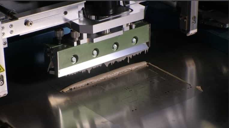
SMT Solder Paste Printing
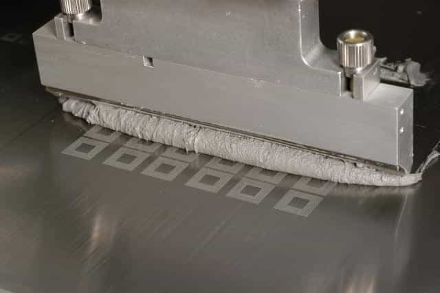
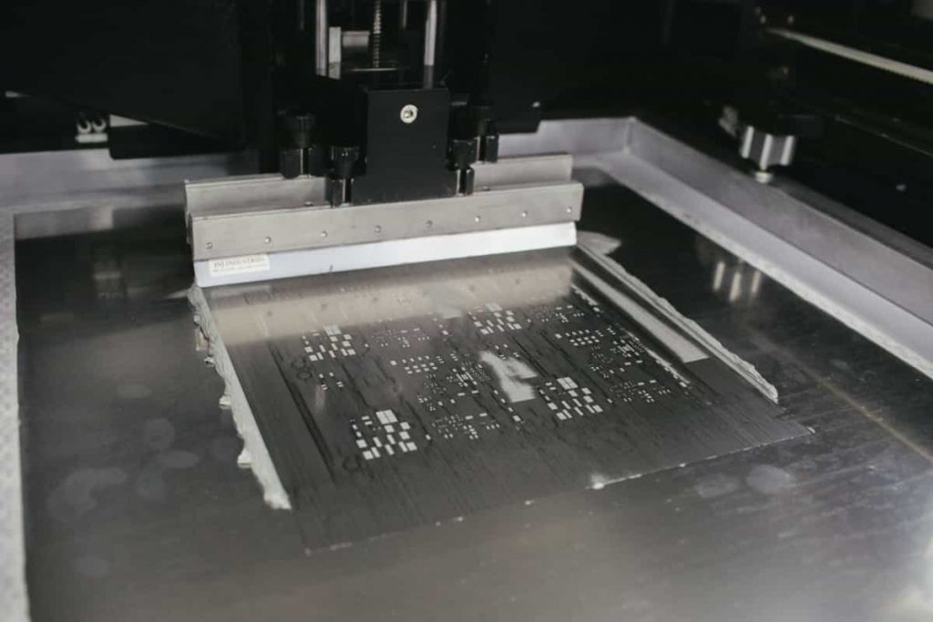
Solder paste printing refers to printing solder paste on the printed circuit board to connect electronic components, which seems like painting on walls. The quality of solder paste printing is vital for the soldering of the PCB board. PCB manufacturers will use a specific stencil to control the solder paste printing to ensure printing precision.
Solder paste printing decides whether the soldering of a printed circuit board is good or bad. With improper printing, it will cause the solder to short and solder empty in soldering. To achieve a high quality of solder paste printing, many elements should be considered.

- Squeegee
PCB manufacturers should choose proper and suitable squeegee according to the difference of solder paste. But at present, the squeegee in solder paste printing is made of stainless steel.
- Squeegee angle
The best squeegee angle in solder paste printing will be 45-60°.
- Squeegee pressure
Squeegee pressure will affect the volume of solder paste on the surface. In principle, under other conditions remain unchanged, the higher the squeegee pressure is, the lower solder paste volume will be.
- Squeegee speed
Squeegee speed will influence the shape and volume of solder paste, which directly decides the printing quality.
- Stencil stripping speed
If the stencil strip speed is too fast, it cannot keep the smooth surface and easy to causes the brush problem, resulting in the bad performance in surface mounting.
- Vacuum block
Vacuum block can help PCB board lie flat on the fixed position, enhancing the compactness between stencil and PCB board. Sometimes, vacuum blocks can be replaced by a universal pin or block to manufacture low-volume disposable products.
- Warpage of PCB
The warpage of printed circuit board will result in the uneven solder paste printed surface, which is more likely to cause the short circuit.
PCB SMT stencil – for accurate solder paste application
PCB stencil is also called SMT Stencil, a specific mold for SMT. PCB stencils help apply solder paste to PCB boards during the reflow soldering process to transfer the exact amount of solder paste to the precise location on the circuit boards. The stencil is placed on the surface of the PCB, and then the solder paste is applied.
PCB stencils are usually created from the duplicate design files with manufacture the PCB. If using the Gerber file, the Top Paste (.GTP) and Bottom Paste (.GBP) files will be used.
The original stencil was made of iron/copper, but later stainless steel replaced them, which is now the stencil (SMT Stencil). According to the production process, the SMT stencils can be divided into Laser Stencil, E.P. Stencil, E.F. Stencil, Step Stencil, Bonding Ni.P. Stencil, and Etch Stencil. Stencil production processes are chemical etching, laser cutting, electroformed.
The thickness of the stencil determines the paste density. The typical thickness includes 0.12mm and 0.15mm.
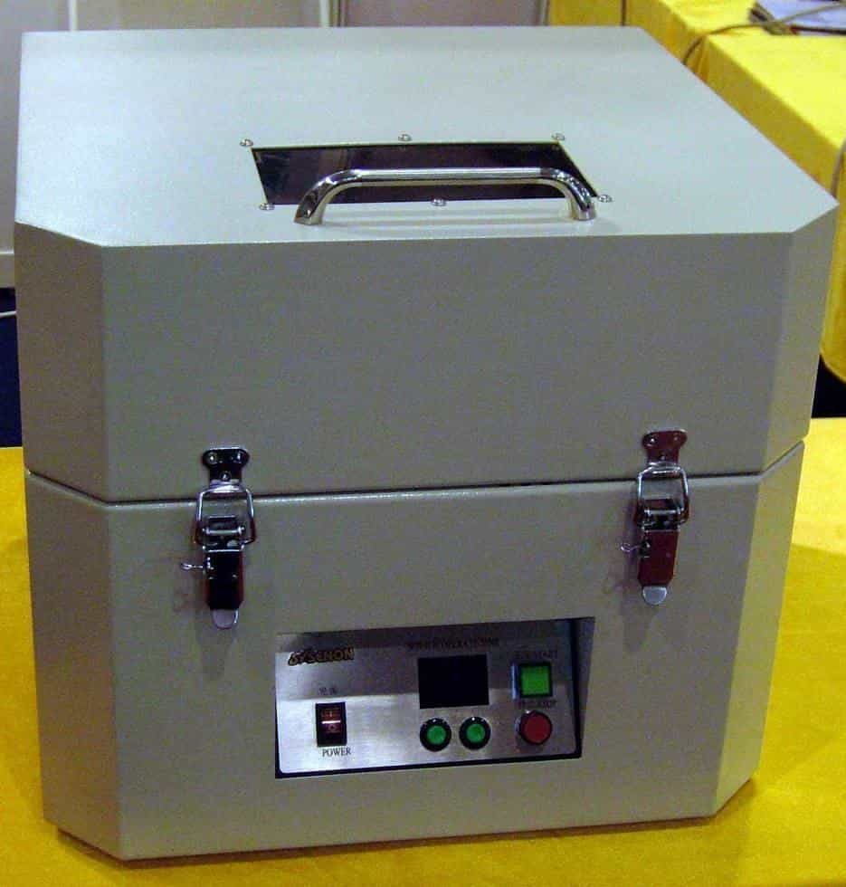
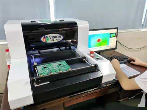
How to inspect the solder paste?
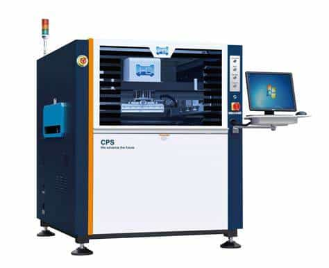
Solder paste inspection is the critical process in the SMT PCB board assembly process, and it is the quality assurance for the finished products. And solder paste inspection is unable to be achieved by manual inspection so it needs the help of solder paste inspection machines to make it. Through the inspection, PCB manufacturers aim to reduce the defective rate in SMT assembly and ensure high quality.
Generally, 80% of defective products in SMT assembly results from improper solder paste printing. That’s why solder paste inspection is becoming more and more critical. And how solder paste inspection plays its role in SMT?
Solder paste inspection machine is only able to operate the surface image check with the inspected area uncovered. And in surface image checking, it will measure and record the following data to tell whether the solder paste printing is good or not, like the height, area, volume, and evenness of solder paste printing. With this data, the solder paste inspection machine will tell whether there is a shift, height deviation, bridge, or solder paste printing damage.
Solder paste inspection plays an essential role in guaranteeing the quality of solder paste printing in the SMT PCB assembly process. All the PCB boards from PCBELEC.COM are done with solder paste inspection to ensure the high quality of PCB boards.
How to Remove Soldermask from Printed Circuit Boards?
It sometimes happens that some parts are covered with a solder mask, where no solder resist is needed, such as testing points, grounding pads, and assembly pins. However, it does not mean that these boards are useless. There are several safe and reliable methods to remove the extra solder mask: scraping, milling, micro-grinding, and chemical stripping. These most commonly used methods have both advantages and disadvantages.
- Scraping
Scraping doesn’t require unique technology or special settings, but it’s a noisy method. Generally, a skilled technician can remove the solder mask from unwanted areas just with a knife, scraper, or chisel. However, if the unwanted areas are large, the operator will feel tired. So it is commonly used for the removal of the thin solder mask layer. This method can be used with other ways to clear the solder mask in the last step.
- Milling
Have you ever used a milling machine to remove the solder mask? It seems extreme, but it is a very efficient and accurate method for removing solder masks. Because of using a sharp cutter, the accuracy must be controlled. The milling system should be equipped with a microscope for visual assistance. Carbide vertical milling cutter is the most commonly used tool because it is sharp and can quickly enter the coating and reach the board’s surface. The opposite direction to turn round cutters is an effective way to control the depth, and the skills and experience are critical.
- Micro-grinding
This is the best technology for removing solder masks in a large unwanted area on the circuit board. In the market, there are several small desktop systems to remove the solder resist. Using a pencil-like handpiece, abrasive material will be moved forward. The abrasive material rubs the solder mask layer. The primary step of this process is friction, and thus will produce an electrostatic charge. If the circuit boards are equipped with electrostatic sensitive devices, the micro-grinding system must eliminate potential electrostatic damage. To remove the abrasive material on the circuit board, it must be thoroughly cleaned.
- Chemical Stripping
This method is the most effective way to remove the solder resist on the copper surface. The stripping area should be isolated to the other parts of the circuit board surface. And then, apply the chemical stripping agent with a brush or cotton swab. Since the stripping agent is liquid, it is often difficult to control. The chemical agent will erode and decompose the solder mask. A chemical stripping agent generally comprising dichloromethane is a potent solvent. Dichloromethane cannot only quickly remove the solder mask. If the delay time is too long, it will also erode the substrate. For these reasons, the chemical stripping agent must be very carefully used.
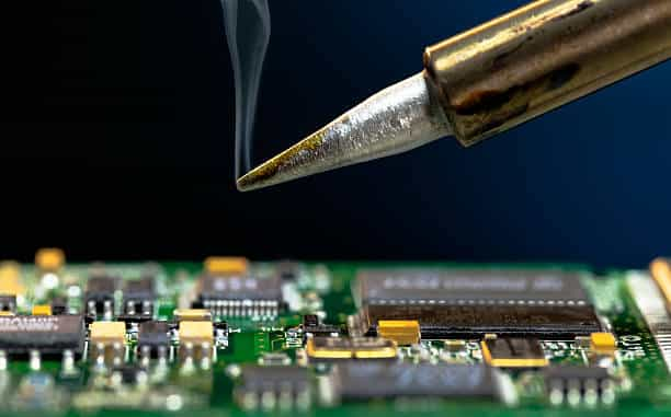
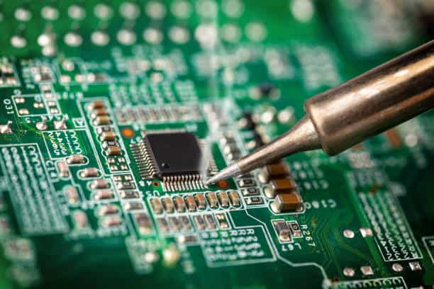
Soldering Irons in PCB Soldering
There are many tools in the soldering process, but none are more critical than the soldering irons. If nothing else, you need at least an iron and some solder to finish the soldering. Soldering irons come in various ways and range from simple to complex, but they all function roughly the same.
Here are some essential factors that make up a soldering iron.
Soldering Tips – No soldering iron is complete without an iron tip. The tip is the iron that heats up and allows the solder to flow around the connected two components. The information transfers heat to raise the metal components’ temperature to the solder’s melting point, with solder melting accordingly. Most irons are removable if users want to replace an old tip or if they need to change the different sizes of the information.
Wand – The wand is the part to hold the tip, which is also the part that users handle. Rods are usually made of various insulating materials (like rubber) to prevent the tip’s heat from transferring to the outside of the wand. Still, they also house wires and metal contacts that move heat from the base or outlet to the tip.
Base – The base typically comprises a large transformer and several other control electronics that safely allow users to adjust temperatures. The wand attaches to the bottom and receives its heat from the electronics inside.
Stand – The iron stand is what places the iron when it is not in use. The air may seem trivial, but leaving an unattended iron laying around on your desk or workbench is a potential hazard: it could burn you, or, worse, it could burn your desk and start a fire. Besides, this helps users prevent the wearing of your tip over time.
Several Through-Hole PCB assembly Soldering Methods
Through-hole technology almost completely replaced earlier electronics assembly techniques such as point-to-point construction. From the second generation of computers in the 1950s until surface-mount technology (SMT) became popular in the late 1980s, every component on a typical PCB was a through-hole component.
What is Through-hole technology in PCB assembly?
Through-hole technology refers to the mounting electronic components, which involve the use of leads on the components inserted into holes drilled in the printed circuit board (PCB) and soldered to pads on the opposite side, either manual assembly or by the use of automatic insertion mount machines.
A variety of through-hole parts with two leads, like resistors, capacitors, and diodes, is done by bending the leads 90 degrees in the same direction, inserting the part in the board, soldering the leads, and trimming off the ends. Tips may be soldered either manually or by a wave soldering machine.
Through-hole technology almost entirely takes the place of earlier electronics assembly techniques such as point-to-point construction. Before surface mount technology became popular in the late 1980s, every component on a typical PCB was a through-hole component.
However, through-hole technology increases the cost by requiring many holes to be drilled accurately. It limits the available routing area for signal traces on layers immediately below the top layer on multi-layer boards. The holes must pass through all layers to the opposite side.
Here are several typical through-hole soldering methods:
- Manual Soldering
Manual soldering is suitable for minimal run production. Welding quality depends on the operators’ experience and skills. And it can be improved through training courses and standards.
- Dip soldering
With this soldering method, the operators need to be close to hot solder pot and flux smoke. Thus, this method is more challenging to do, and it is dangerous for the operators.
Advantage: low cost per solder joint, fast soldering speed.
- Wave Soldering
Wave soldering is the most common and effective way. The wave soldering system has a big enough wave soldering tin to handle the maximum expected board width. Wave soldering is usually applied in medium-volume or large-volume PCB soldering.
- Selective Soldering
Selective soldering is a particular soldering method. When some components have been installed on the PCB board, wave soldering cannot be used to install through-hole components so that selective soldering becomes the only way to solder through-hole components on the board.
Advanced Learning:
- The Main PCB Assembly process Steps
- Low Volume PCB Assembly Service
- How To Clean The Solder Paste On SMT Stencil
- What is the difference between SMT and SMD?
- What is the difference between wave soldering and reflow soldering?
- What Is A Surface Mount Device Or SMD Component Package?
- 30 Common SMT PCB Assembly Defects


