With the rapid development of electronic products, components have become smaller and smaller, and the requirements for PCB stencils have become higher and higher. According to different production processes, stencil mainly includes chemical etching, laser cutting, and electroforming. The SMT stencil is primarily composed of a screen frame, wire mesh, steel sheet, and bonding glue.
1. Materials for Making SMT stencil
a) The Screen Frame
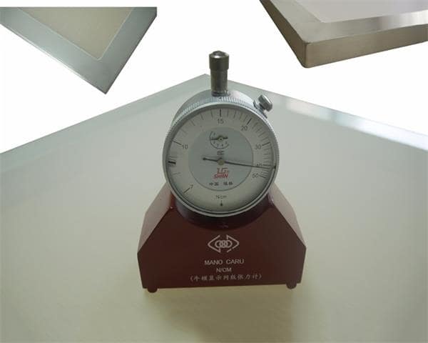
The screen frame is divided into movable and fixed frames. The portable frame directly installs the steel sheet on the frame, and the structure can be used repeatedly. The fixed frame is covered with glue on the screen frame, and later, it is set by bond. The fixed screen frame is easier to obtain uniform steel sheet tension, and the pressure is generally 35~48N/cm2. (Normal limited network allows tension frame 35 Newtons-42 Newtons)
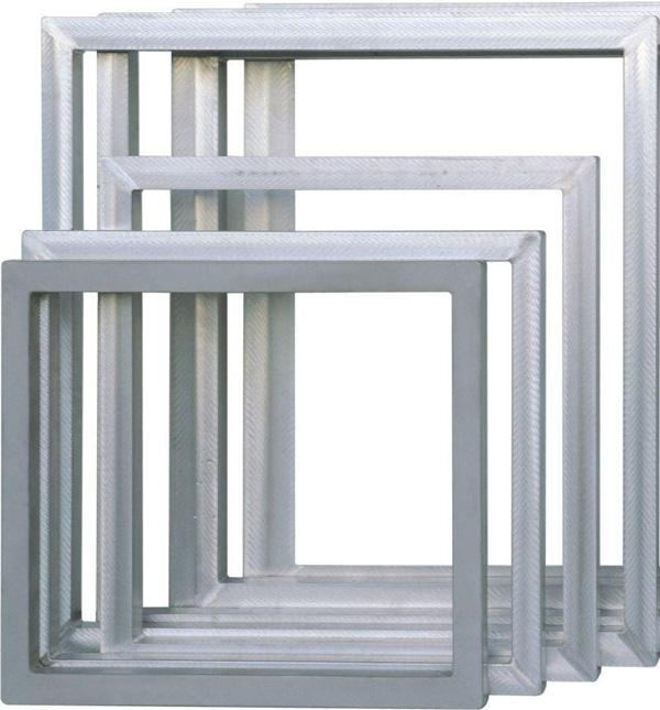
b) Wire Mesh
The mesh screen frame is used to fix the steel sheet and net frame and be divided into stainless steel wire mesh and high molecular polyester net. Stainless steel wire mesh is usually about 100 meshes, which can provide a relatively stable and sufficient tension, but stainless steel wire mesh is easy to deform and lose pressure after a long time of use. The polyester mesh net is often used for an organic matter of 100 mesh, which is not easy to deform and has a long service life.
c) Steel Sheet
Copper sheets, stainless steel sheets, nickel alloys, polyesters, etc., are used to make holes. The template generally adopts a high-quality foreign 301/304 stainless steel sheet, and the foreign steel sheet dramatically improves the service life of the template with its excellent mechanical properties.
d) Glue
The glue is used to stick the screen frame, and the steel sheet has a more significant effect on the template. It can be specially used for different customers’ use conditions. This glue can maintain firm adhesion and can resist various template cleaning agents during complex cleaning.
2. SMT Stencil Production Method
a) Chemical Etching
Process:
PCB Data file(PCB Gerber file)→Film production→Exposure→Development→Etching→Steel Cleaning→Netting.
Features:
- One-time molding
- Faster speed
- Lower price
Disadvantages:
- Easy to form an hourglass shape (not enough etching) or larger opening size (over etching).
- Objective factors (experience, medicament, film) have a significant impact, many production links, and large cumulative errors.
- It is not suitable for the acceptable pitch steel mesh production method.
- The production process is polluted, which is not conducive to environmental protection.
b) Laser Cutting Method
Process Flow:
Film→Coordinates→Data file→Data processing→Laser cutting→Polishing→Encapsulation
Features:
- High precision of data production
- Small influence of objective factors
- The trapezoidal opening is suitable for demoulding.
- It can be used for precision cutting.
- Fair price
Disadvantages: Cutting is one by one, so the production speed is slow.
c) Electroforming Method
Process flow:
Coating photosensitive film on substrate → Exposure → Developing → Electroforming nickel → Forming → Steel sheet cleaning → Packaging
Features: Smooth hole wall, especially suitable for ultra-fine pitch steel mesh production method.
Disadvantages:
- The process is difficult to control.
- The production process is polluted, which is not conducive to environmental protection.
- The production cycle is long
- Price is too high
3. Opening design
The opening design of the stencil should consider the mold release of the solder paste, which is determined by three factors:
- The width to thickness ratio/area ratio of the opening
- The geometric shape of the sidewall of the opening
- The smoothness of the hole wall.
Width to Thickness Ratio: The ratio of the opening width to the thickness of the stencil.
Area Ratio: The ratio of the opening area to the cross-sectional area of the hole wall. Generally speaking, to obtain an excellent demoulding effect, the width to thickness ratio and the area ratio should be greater than 1.5 and 0.66. Never ignore the process issues, such as continuous tin and multiple tins, to achieve aspect ratio and area ratio.
SMT Stencil Opening Design Tips:
- Fine-pitch IC/QFP: The best way to prevent stress concentration is to have rounded corners at both ends. The same is true for BGA, 0402, and 0201 with square holes.
- The anti-tin bead opening method of chip components is best to choose the concave opening method, effectively preventing component tombstones.
- When designing the solder paste stencil, the opening width should ensure that the four most enormous solder balls can pass smoothly.
4. Post-processing
Etching and electroforming SMT solder paste stencils generally do not require post-processing. The circuit board stencil post-processing mentioned here is mainly for laser cutting SMT stencil.
Because the metal slag will adhere to the hole wall and opening after laser cutting, the surface is generally polished. Polishing removes the slag, and it creates friction on the surface. It is done to increase the surface friction for better rolling of the solder paste and obtain an excellent soldering effect. If necessary, you can also choose “Electropolishing,” which has a perfect impact on removing slag (burrs) and improving the hole wall.
Different production processes, raw materials used, and opening design will significantly impact the stencil quality, so it is essential to master the production process and specifications of the solder paste stencil.
Related PCB Assembly Services
- LED PCB Assembly
- Through Hole PCB Assembly
- SMT PCB Assembly
- Fast Prototype PCB Assembly Service
- Low Volume And Quick Turn PCB PCB Prototype Assembly Services
- 10 Tips For PCB Assembly Manufacturing Design
Advanced Learning:


