Table of Contents
Introducing Blank PCBs
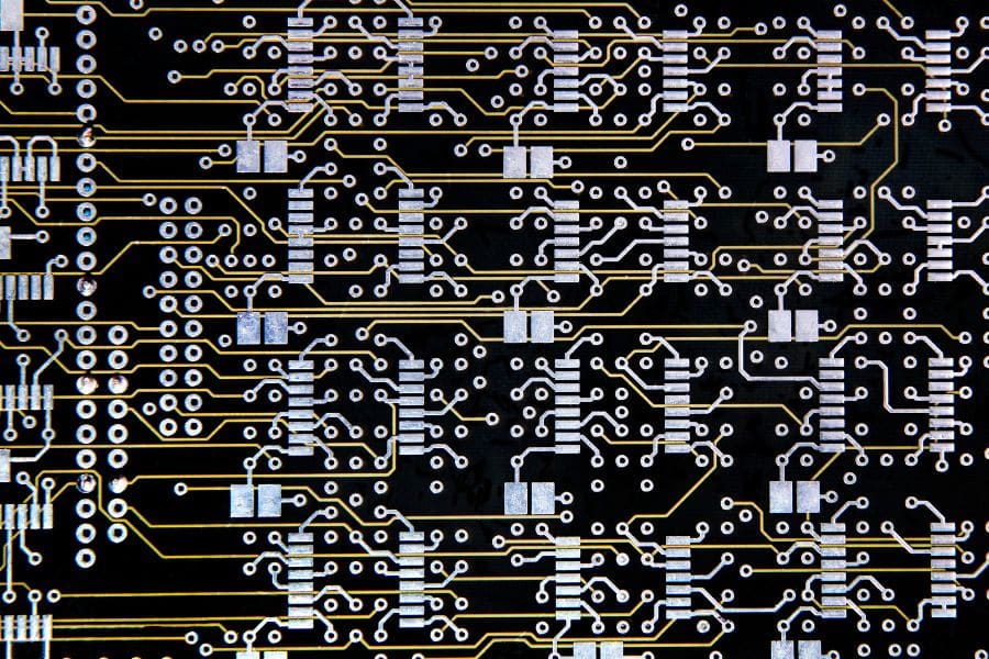
A blank PCB forms the foundation of an electronic circuit before components are soldered onto it. Also referred to as a bare PCB, it is the base board that provides the connections between inputs, outputs and various components in an electronic device.
Understanding what a blank PCB is and its role in electronics manufacturing is important for designing and producing the boards efficiently. In this comprehensive guide, we will cover everything you need to know about blank PCB technology.
A. Definition of a Blank PCB
A blank PCB starts as a non-conductive flat surface, usually made of composite materials like FR-4. Conductive copper layers are then patterned on top, typically through a process called photolithography. The patterned copper layer forms the interconnections between components in line with the circuit diagram requirements.
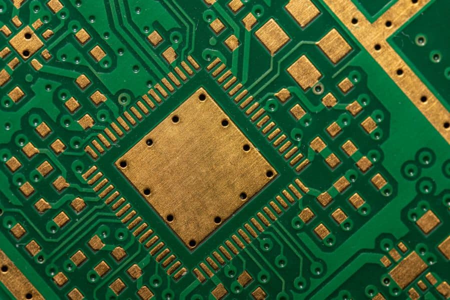
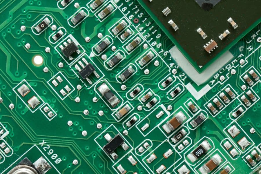
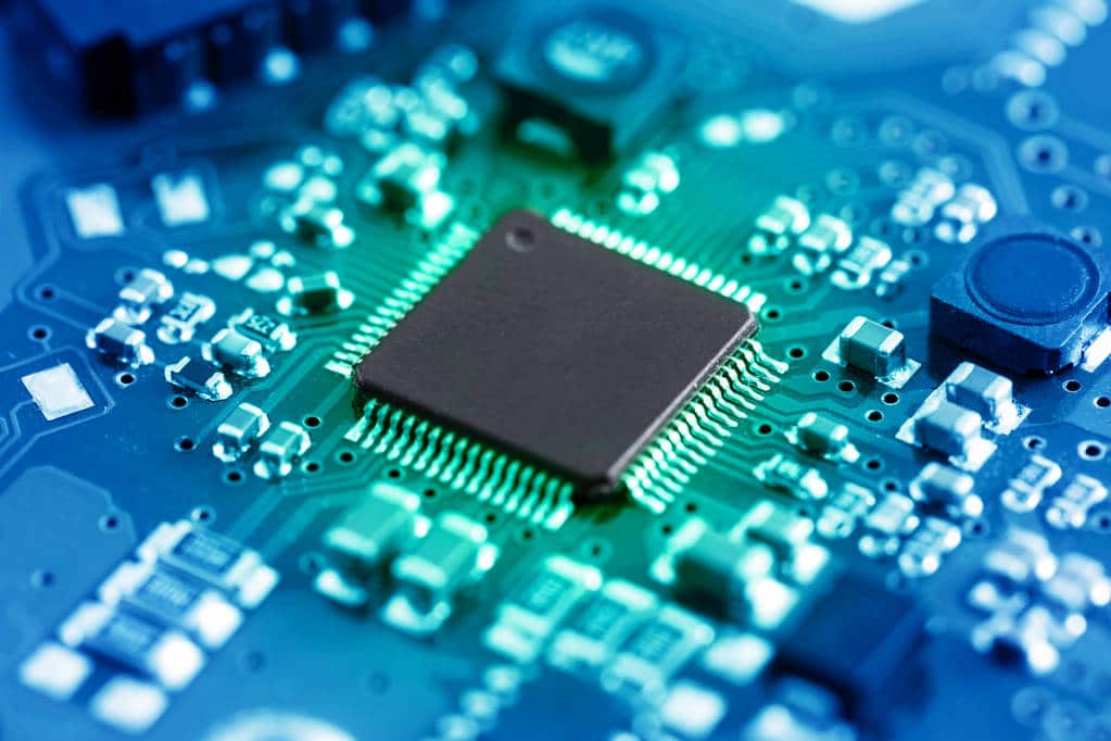
Before components like ICs, resistors or capacitors are soldered onto the PCB, it is known as a “blank” or “bare” board. Blank PCBs can be basic single-sided boards with copper on one side only or complex multilayer boards with over 20 conductive layers.
B. Also Known as Bare PCBs
Blank PCBs are also referred to as bare printed circuit boards due to the fact that they do not yet have electrical components mounted on them. These base boards consist solely of the insulating substrate and conductive copper traces, without any peripherals or devices attached.
The terms blank PCB and bare PCB are often used interchangeably. Some people also use other names like base boards, empty boards or unfinished boards. But these unfinished boards are called blank or bare PCBs in most manufacturing and design documentation.
C. Base for Building Circuit Boards
Blank PCB boards form the platform on which all circuit components like processors, capacitors, switches, and chips are assembled. The layered copper interconnects provide the conduction pathways between different components. This allows efficient transmission of power and signals in line with the intended circuit functions.
Higher-layer blank boards also integrate contacts and communication interfaces like USB ports or display connectors during fabrication. This facilitates integration during PCB assembly or device manufacturing downstream based on requirements. Understanding blank PCB capabilities and manufacturing processes enables developing electronic products better.
Benefits of Using Blank PCBs
Blank PCB manufacturing offers significant advantages compared to assembling circuits on perf boards or using strip boards for prototyping. Their benefits make blank PCBs integral to modern electronics design and production.
A. Flexibility and customization for Multiple Designs
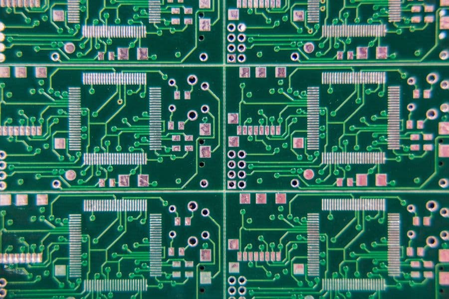
Since blank circuit boards can be fabricated according to varied circuit requirements, they provide extensive flexibility. The blank PCB manufacturing process can produce boards with anywhere from single-sided to over 32 conductive layers. This facilitates integrating complex circuits cost-effectively.
They are also not restricted in size or shape either during designing or manufacturing. Rectangle blank PCBs are common but circular, triangular or oddly shaped boards can also be produced depending on mechanical requirements. This design flexibility enables fitting PCBs seamlessly across various devices and packages.
Having blank PCB boards manufactured rather than assembling circuits manually provides extensive customization capabilities too. This allows incorporating the exact circuit pathways, interconnect densities, heat sinks and interfaces needed.
B. Cost Savings
Producing blank printed circuit boards, especially through high-volume manufacturing, brings significant cost savings over manual approaches. The economies of scale combined with efficient fabrication processes reduces overall costs.
Since volume manufacturing amortizes fixed infrastructure and labor costs, each blank PCB board becomes cheaper to produce. This allows companies to maintain margins while selling devices incorporating PCBs cheaper. The cost savings can also be utilized to provide more product features improving competitiveness.
C. Faster Time to Market
Blank PCB manufacturing also enables bringing electronic products faster to market. Instead of having to manually design and assemble multiple prototypes, most design validation and testing can be done on manufactured blank boards itself.
Any issues with the circuits or board can be identified within a few iterations before commencing final production. This avoids costly delays due to prototyping issues. Blank PCBs thus help accelerate the product development life cycle considerably.
D. Enables Prototyping & Testing
Having blank PCB boards manufactured provides an effective platform for testing out circuit designs through prototyping iterations. Multiple design ideas can be quickly iterated on fabricated blank boards instead of manual perf board builds.
This prototyping verifies circuit functionality, thermal performance, signal integrity, and interference aspects. Any issues found during prototyping on blank boards can be addressed before finalizing the design. This ensures the production PCB circuitry and layout works as intended.
Blank boards thus increase development productivity significantly through enabling iterative prototyping. They allow design flaws to be identified early saving considerable time and development costs.
Blank PCB Components
While blank printed circuit boards may seem simple from the outside, they comprise multiple materials and components engineered precisely to function as intended. Understanding the constituent components that make up a blank PCB is important.
A. Substrate Materials Like FR-4
The base substrate material forms the foundation on which circuits are built in a blank PCB. FR-4 glass epoxy is the most commonly used substrate thanks to its favorable electrical and mechanical characteristics. Alternatives like CEM-1 may be used for certain high-frequency or flexible PCBs.
The substrate insulates the conductive copper layers from each other preventing short circuits while enabling formation of trenches and vias. The dimensional stability of materials like FR-4 also enables creating fine circuit patterns and holding embedded components reliably.
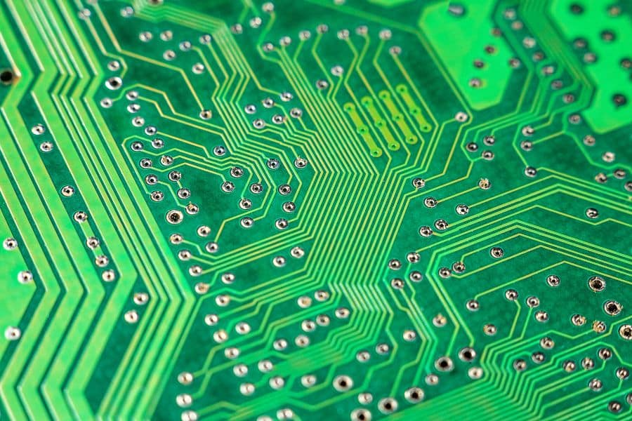
B. Layers – Single, Double, Multi-layer
Based on circuit complexity, blank PCBs can incorporate anywhere from a single copper layer to over 20 conductive layers that are interleaved using the substrate. For a single-layer blank board, the substrate forms the bottom layer with only the top side having etched copper.
In double or multi-layer boards, multiple copper layers are separated using substrate core material for insulation. Blind and buried vias help interconnect the inner layer traces for complex compact designs.
C. Stackup – HDI, High Frequency
The arrangement of conductive layers interleaved with substrate cores is known as the board stackup. Along with the number of layers, properties like thickness, material and copper weight also characterize the stackup.
For example, boards intended for very high-density interconnects utilize thinner cores and denser stacks with more layers. Similarly, high-frequency blank PCBs require stackups with tightly controlled impedances that match component requirements.
D. Finishes and Coatings
While not part of the functional circuit layers, finishes and coatings play a critical role in blank PCB durability, solderability and aesthetics. Common finishes include:
- Hot Air Solder Leveling (HASL) using tin-lead or lead-free alloys provides enhanced solderability and shelf life.
- Immersion Silver and Immersion Tin finishes avoid oxidation improving solder joint integrity.
- Gold plating of contact fingers and connectors improves conductivity and corrosion resistance.
- Protective nickel/gold coatings shield copper traces from environmental damage.
- Conformal coatings safeguard against contamination or leakage currents.
Blank PCB Design Considerations
Creating the circuit layout and board design for a blank printed circuit board needs careful considerations across various aspects. These include schematic planning, layout software capabilities, layer stackup decisions and manufacturability guidelines.
A. Schematic Circuit Draft
The first step is drafting the schematic diagrams depicting circuit connectivity requirements using PCB design software. All elements like ICs, discrete components, interfaces and terminals are mapped along with their electrical relationships.
Software performs netlist extraction and component placement planning from completed schematics before layout. Planning schematics with sound PCB design practices in mind eases subsequent stages.
B. PCB Layout Software Rules
Modern PCB layout tools incorporate extensive rule checks during routing and layout stages alerting to violations. This helps designers avoid issues like insufficient spacing between components or traces based on board capabilities.
High-density blank PCBs require following more stringent design rules to facilitate fabrication and assembly. Factoring in appropriate tolerances during layout enhances material utilization also minimizing costs.
C. Layer Stackup Configurations
The conductive layer types, sequence, properties and vias linking them characterize the stackup. Optimized stackups tailor blank PCB capabilities to circuit needs with adequate power/ground planes and signal routing layers.
Modeling software simulation also validates electrical, thermal and mechanical performance for chosen blank board stackup configurations before fabrication. This minimizes risk of issues during testing prototypes.
D. Design for Manufacturing Guidelines
Besides the circuit functionality itself, optimizing designs to facilitate manufacturing is vital for fabricating blank PCBs efficiently. Guidelines regarding minimum feature sizes, tolerances, component spacings and copper weights help streamline fabrication. Considering capabilities of target PCB manufacturers regarding line width, registration and finishes also ensures ability to procure boards with required quality later. Designing blank boards amenable to automated assembly also reduces long-term costs.
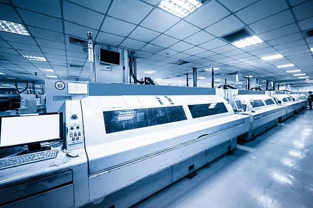
Blank PCB Manufacturing Process
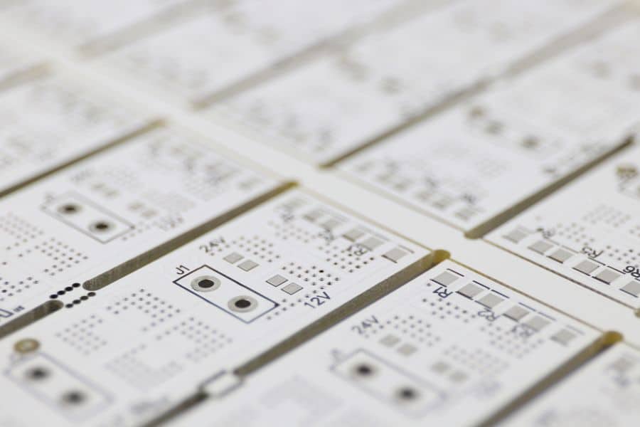
Blank PCBs can be fabricated in lower volumes for prototyping needs or mass produced for supporting production requirements. The complex manufacturing process involves sourcing suitable materials followed by multiple fabrication stages to realize the board design. Key process steps include:
A. Prototyping vs Production
Prototyping blank PCB fabrication aims for faster turnaround focusing on validating functionality. Production optimization targets higher yields through process refinement while minimizing costs. Achieving both goals requires tight coordination between design and manufacturing teams.
B. Sourcing Quality Raw Materials
High-purity base materials, including laminates, copper foils, glasses, resins and more are sourced from reliable suppliers in line with design requirements. Stringent sourcing standards ensure consistency and traceability of raw materials feeding PCB fabrication.
C. Panel Cutting and Preparation
Fabrication starts with cutting substrate laminates into panels as per board dimensions followed by processes like bevelling, drilling and surface treatment to ready panels. Automated optical inspection verifies panel quality before imaging.
D. Imaging and Etching Copper Layers
Next, photoresists are coated on panels to transfer circuit patterns using lithographic techniques. Acid etching then removes copper from undesired areas while retaining intended interconnects. Repeated across layers, this builds up the designed conductive network.
E. Drilling Holes and Vias
High-precision drilling machines create thousands of holes and vias across the panel to facilitate component mounts and layer interconnects conforming to layout data. Deburring removes residues preparing the holes for metallization.
F. Plating, Coating and Finishing
To facilitate soldering and protect copper traces, a series of plating, coating and finishing processes are executed. These include electroplating, screen printing, vacuum deposition and more to build up metallic and organic protective layers as needed.
G. Electrical Testing
Post-fabrication, automated flying probe, and bed-of-nails testers validate board connectivity, continuity and functional performance through extensive testing. This screening catches defects prior to shipment ensuring consistent quality to consumers.
H. Quality Assurance
Besides inline process inspection at all stages, finished boards undergo meticulous visual QC audits based on stringent acceptability criteria. This oversees all attributes guaranteeing delivery of flawless blank PCBs to destinations. Environmental stress screening also validates robustness.
Types of Blank PCBs
Blank PCBs can be fabricated in different forms and materia3constructions to serve varied electronic product needs – from rigid boards for structural stability to flexible ones for withstanding vibrations. Some key varieties include:
A. Rigid Circuit Boards
The most common blank PCB type, rigid boards provide maximal mechanical strength and ease of assembly for electronic circuits. Their dimensional stability also suits high-density component mounting. FR-4 glass epoxy substrate is commonly employed although alternatives like CEM-1 may also be used.
B. Flexible Boards
Flexible PCBs use thin insulating polymer substrates that can bend and twist enabling innovation designs not feasible previously. Common flexible blank board materials include polyimide, PET, PEN or other plastic films combined with adhesive copper foil. Protective coatings safeguard against environmental factors.
C. Rigid-Flex Boards
Where mechanical compliance as well flexibility is needed simultaneously, rigid-flex PCBs integrate both capabilities. Multilayer rigid sections provide stability and mounting surfaces while thinner flex portions accommodate bends through form-factors. These provide best of both worlds.
D. HDI Boards
To integrate complex digital processors and packing high density of interconnects, High-Density Interconnect or HDI PCBs became vital for miniaturization. These utilize thinner dielectrics while stacking more conductive layers with smaller vias and traces enabling dense component mounts.
E. Special Materials Boards
Rarely, PCB substrate may use alternate insulating materials for specialized applications – ceramic packages for transistors, Teflon resins for high temperatures or in automotive running at higher voltages applications. Maximizing capability requires choosing optimal blank board raw materials.
Applications of Blank PCBs
The versatile blank PCB manufacturing capabilities today enables their widespread adoption across a diverse range of electronics products and domains including:
A. Consumer Electronics
From smartphones to laptops, tablets to home appliances and gaming consoles, printed circuit boards permeate across consumer electronics. High volume production paired with compact form factors and robust quality levels makes this the leading PCB application today.
B. Industrial Electronics
Machinery controls, robotics, power conversion and monitoring systems utilized in factories routinely employ PCBs customized to requirements. Tolerating higher temperatures and vibrations with noise immunity often requires fabrication process refinements.
C. Automotive Electronics
Modern connected cars maybe incorporating over a thousand blank PCBs customized for efficiency, safety and comfort applications. Stringent quality needs given harsh under-the-hood environments and longevity needs of vehicles necessitates specialized PCB fabrication.
D. Aerospace and Defense
Ruggedized avionics systems and navigation electronics in aerospace applications utilize specially processed boards that withstand extreme altitude and temperature variations reliably over decades. Defense electronics similarly demand specialized blank PCBs meeting strict specifications.
E. Medical Devices
Life critical medical instruments and implantable devices as pacemakers have stringent electronic performance needs combined with demanding size, biocompatibility and reliability needs that custom blank PCB fabrication aims to achieve.
F. IoT and Wearables
The booming internet-of-things and wearable categories also increasingly adopt PCB advancements enhancing capabilities while minimizing size and cost. This expanded adoption will further fuel PCB innovation across application categories in the future.
Sourcing High Quality Blank PCBs
Procuring blank printed circuit boards meeting quality, reliability and consistency expectations requires careful evaluation and selection of the right PCB manufacturing partner.
A. Research and Qualify
PCB Manufacturers The first step is to thoroughly research capabilities of promising PCB producers based on product needs while factoring in cost impact. Developing a vendor shortlist through online searches coupled with peer recommendations helps. Onsite audits must then quantify manufacturing infrastructure, quality procedures and consistencies.
B. Evaluate Capabilities, Expertise and Services
The stringent requirements like sophisticated processes, material handling or complexity management for advanced PCBs necessitates manufacturers having state-of-the-art fab infrastructure and expertise built through years of focused learning. Supplementary value-added services in terms of engineering support or logistics also aids. Holistically evaluating capability metrics helps determine the right partner.
C. Quality Certifications – ISO, IATF
Stringent international quality management certifications such ISO 9000 or automotive focused IATF 16949 point towards comprehensive quality frameworks addressing all aspects-from product realization to customer satisfaction. Such unbiased third-party audited certifications help identify competent fabrication partners.
D. Reliable Delivery and Support
Consistently meeting quoted lead times with reliable logistics for both lower volume prototyping and scaled up production runs is imperative. Managing a collaborative relationship through effective issue resolution and technical support also minimizes product development risks for a smooth partnership.
Conclusion and Summary
A. Recap Blank PCB Definition and Benefits
To conclude, blank printed circuit boards or bare PCBs constitute the backbone enabling electronics innovation through their unmatched capabilities to pack complex and reliable circuitry in highly customizable and cost-effective manner. Their benefits and fabrication will only expand further as technology progresses.
B. Key Takeaways for Designing and Sourcing
The essentials of blank PCB capabilities and manufacturing stages allows for optimizing electronics designs taking all interdependencies into account right from conceptualization. Carefully evaluating PCB manufacturing partners based on rigorous quality frameworks ensures actualizing designs to products dependably.
C. The Future of Blank PCB Technology
Ongoing PCB advances enabling integrating more layers, smaller features reliably through process innovations positions blank PCB fabrication to support exponentially growing electronics application complexity needs over coming decades.
JHYPCB - Your Dependable Blank PCB Manufacturing Partner
Headquartered in China, JHYPCB has over 14 years of expertise specializing in efficient fabrication of high-quality blank PCBs at scale leveraging smart manufacturing 4.0 infrastructure. With robust quality assurance and certification frameworks guaranteeing excellence along with value-added engineering support, JHYPCB delivers exceptional service as your trusted PCB manufacturing partner.


