Table of Contents
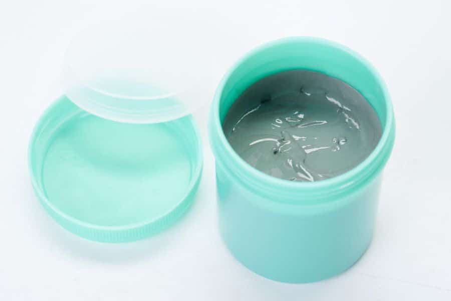
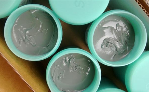
What is Lead-Free Solder Paste?
Lead-free solder paste is a type of solder material used in electronic assemblies that does not contain lead. Traditional solder pastes contained a tin-lead alloy, with lead concentrations around 40%. However, due to environmental and health concerns over the toxicity of lead, legislation has been passed restricting the use of lead in electronics manufacturing.
The key requirement for lead-free solder pastes is that the lead content must be below 0.1% or 1000 ppm. This extremely low threshold essentially eliminates lead as an ingredient. Instead, lead-free solder pastes utilize alloys of tin combined with other metallic elements like silver, copper, bismuth, antimony, etc.
The move towards lead-free soldering has been driven by regulations like the European Union’s RoHS directive. RoHS aims to limit the use of certain hazardous materials, including lead, in electrical and electronic equipment. As a result, the electronics manufacturing industry has had to transition to lead-free solder paste and lead-free assembly processes.
The development history of lead-free solder paste
The transition to lead-free solder pastes has been an ongoing process over the past few decades. Initial efforts to restrict the use of lead in electronics faced pushback from the industry in the early 1990s when the US Senate proposed limiting lead content to below 0.1%.
However, research into viable lead-free alternatives continued, with organizations like NEMI, NCMS, NIST and others investing over $20 million into studying lead-free solders through the 1990s. Japan was an early mover, revising its household electronics recycling law in 1998 to drive the development of lead-free products.
Major milestones included the first mass-produced lead-free electronic product from Matsushita in October 1998. The US IPC and Japanese JEITA then published lead-free roadmaps in 2000 and 2002 respectively, recommending electronics companies transition fully to lead-free by 2004-2005.
The most significant driver was the European Union’s RoHS directive in 2003, which banned the use of lead and other hazardous substances in new electrical and electronic products sold in the EU market from July 2006 onwards. This regulation spurred a global shift to lead-free soldering across the electronics supply chain.
- 1991 and 1993: The US Senate proposed limiting the lead content in electronic solders to below 0.1%, which was strongly opposed by the US industry and failed.
- From 1991: Organizations such as NEMI, NCMS, NIST, DIT, NPL, PCIF, ITRI, JIEP successively launched special research on lead-free solders, spending more than $20 million, which is still ongoing.
- 1998: Japan revised the Household Appliance Recycling Law, driving companies to develop lead-free electronic products.
- October 1998: Matsushita released the first mass-produced lead-free electronic product.
- June 2000: The US IPC’s Lead-Free Roadmap 4th edition was published, recommending US companies introduce lead-free electronic products in 2001 and achieve full lead-free by 2004.
- August 2000: Japan’s JEITA Lead-Free Roadmap 1.3 was published, recommending Japanese companies achieve standardized lead-free assembly by 2003.
- January 2002: The EU Lead-Free Roadmap 1.0 was published, providing important statistics on lead-free adoption based on a survey.
- January 23, 2003: The European Parliament and Council issued Directive 2002/95/EC on restricting hazardous substances in electrical and electronic equipment, clearly defining six substances including lead that must be restricted. It mandated that from July 1, 2006, electronic products sold in the EU market must be lead-free (with some exemptions).
Importance and applications of lead-free solder paste
The transition to lead-free solder pastes has been driven primarily by environmental and health concerns over the toxicity of lead. Lead exposure can cause significant health issues, especially in children where it can impact brain development and intelligence. It can also create environmental contamination issues through improper disposal of lead-containing electronics waste.
Adopting lead-free solder is therefore an important step in making electronics manufacturing more sustainable and environmentally-friendly. The RoHS directive and similar legislation around the world aims to minimize the use of hazardous substances like lead across the entire electronics supply chain and product lifecycle.
Lead-free soldering is now a requirement for any company manufacturing electronics products to be sold in the European Union, United States, China and many other major markets. It impacts a wide range of consumer and industrial electronic devices including computers, mobile phones, home appliances, automotive electronics and more.
In addition to assembly of new electronics, lead-free solder paste is also commonly used in repair and rework processes on existing products to maintain RoHS compliance. Overall, transitioning to lead-free soldering has been a crucial environmental initiative for the global electronics manufacturing industry over the past 20 years.
The main components of lead-free solder paste
The primary components of lead-free solder pastes are alloys made up of tin combined with smaller amounts of other metallic elements like silver and copper. The most widely used lead-free solder alloy is the tin-silver-copper (Sn-Ag-Cu) system.
In this ternary Sn-Ag-Cu alloy, the metallurgical reactions between tin and the minor elements silver and copper govern key properties like melting temperature, solidification behavior, and mechanical strength. According to binary phase diagrams, there are three potential eutectic reactions between the three elements.
Tin and silver form a eutectic at 221°C consisting of a tin matrix and the intermetallic Ag3Sn compound phase. Tin and copper form a 227°C eutectic of a tin matrix with the intermetallic Cu6Sn5 compound. Silver and copper also have a higher 779°C eutectic between their solid solution phases.
However, research indicates the ternary Sn-Ag-Cu system likely involves silver and copper reacting directly, favoring formation of the Ag3Sn and Cu6Sn5 intermetallic compounds within the tin matrix microstructure. These relatively hard intermetallic particles effectively strengthen the tin-based alloy through dispersion and internal stress fields.
The finer the dispersion of the intermetallic particles, the smaller and more refined the overall microstructure, improving mechanical properties like creep resistance. Typical Sn-Ag-Cu lead-free solder compositions contain 3-4% silver and 0.5-1% copper by weight.
While silver and copper levels are important, the melting temperature is not highly sensitive to variations within these ranges. Higher silver increases strength but reduces ductility, while copper above 1.5% can decrease yield strength. An optimum combination is around 3% Ag and 1-1.5% Cu.
The key technical requirements for lead-free solder pastes
Lead-free solder pastes must meet several critical technical criteria to ensure high performance and reliability in electronics assembly:
- Low Melting Point
The melting point should be as close as possible to the 183°C eutectic of traditional 63/37 tin-lead solder. While no true lead-free eutectic alloy exists yet, the melting range between solidus and liquidus should be minimized, with a maximum liquidus around 225-230°C for SMT assembly. - Good Wetting Ability
Whether for wave, reflow, or selective soldering, the solder paste must exhibit excellent wetting on component leads/pads and board surfaces within the short time liquid phase during heating cycles (typically 30-90 seconds reflow, 4 seconds wave). - Electrical/Thermal Conductivity
The joint conductivity and ability to transfer heat away should be comparable to tin-lead solders. - Mechanical Strength & Ductility
Solder joints require sufficient tensile strength, creep resistance, ductility and resistance to thermal fatigue stresses over the product lifetime. - Cost-Effectiveness
While higher than tin-lead, the raw materials cost should be controlled to around 1.5-2x the cost of conventional solder paste. - Compatibility
The solder paste must wet and interact appropriately with board finishes, component metallizations, and flux systems – working with both resin and resin-free formulations. - Inspection & Rework
Post-assembly inspection, testing and any rework/repair procedures should be feasible. - Materials Availability
The elemental constituents must have reliable long-term availability and supply. - Compatibility with Processes/Equipment
Adoption should require minimal changes to existing soldering processes and equipment.
Meeting all these criteria is an ongoing challenge, but essential for lead-free solders to provide equivalent performance to tin-lead solders across different assembly processes.
The different classifications of lead-free solder pastes
Lead-free solder pastes can be categorized in several ways based on their formulation and characteristics:
By Flux Type
– Rosin/Resin-Based (RA) Pastes – Contain rosin or synthetic resin activators for good wetting
– No-Clean or Residue-Free (RF) Pastes – Designed to leave minimal residues after reflow
– Water-Soluble (OA) Pastes – Use organic acid activators that can be cleaned with water
By Reflow Temperature Range
– High Temperature (HT) Pastes – Liquidus over 230°C, e.g. SAC305 (96.5Sn/3Ag/0.5Cu)
– Mid Temperature (MT) Pastes – Liquidus 217-230°C, e.g. SAC387 (95.5Sn/3.8Ag/0.7Cu)
– Low Temperature (LT) Pastes – Liquidus below 217°C, often containing bismuth
By Alloy Composition
– SAC Alloys (Tin/Silver/Copper) – Most common Pb-free composition, e.g. SAC305, SAC387
– SAC-Bi Alloys – Add bismuth for lower melting points, e.g. SACm®0510 (97.4Sn/3Ag/0.5Cu/1Bi)
– Low/No-Silver Alloys – Use alternate dopants like copper or nickel, e.g. SN100C® (98.5Sn/0.5Cu/0.05Ni)
The choice depends on the application, temperature requirements, residue preferences and cost factors. SAC alloys dominate for RoHS compliance, with lower temperature or no-silver alloys offering niche alternatives.
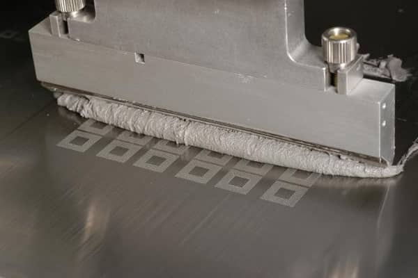
Many lead-free solder pastes are also halogen-free to be more environmentally-friendly. Proper paste selection is critical to ensure good printability, consistent reflow performance and long-term solder joint reliability.
Applications of lead-free solder paste in electronics manufacturing
- Lead-Free Solder Paste in Electronics Assembly
As a leading Chinese PCB manufacturer, JHYPCB provides comprehensive lead-free PCB assembly services to meet RoHS and other environmental compliance requirements. Our lead-free assembly capabilities include: - Turnkey Lead-Free PCB Assembly
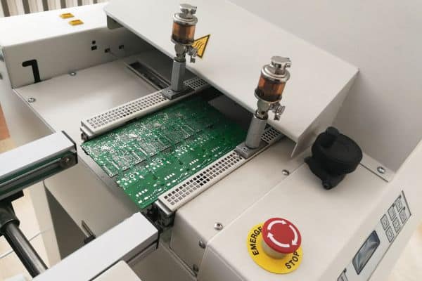
We offer full turnkey lead-free assembly for both SMT and through-hole components utilizing lead-free solder pastes and lead-free reflow and wave soldering processes. - SMT Lead-Free Assembly
For surface mount assembly, we use lead-free no-clean and rosin-based solder pastes qualified for small passive components up to large BGA/CSP packages. Our SMT lines are optimized for lead-free reflow with controlled heating profiles. - Through-Hole Lead-Free
For through-hole and mixed-technology assemblies, our wave soldering systems are set up for lead-free wave soldering using lead-free solder pastes and lead-free solder baths. - Low-Cost Lead-Free Solutions
We offer highly competitive lead-free PCB assembly pricing without compromising on quality or reliability. Our lead-free solutions minimize costs through efficient processes and volume pricing.
As a one-stop lead-free PCB assembly provider, we work closely with our customers to select the optimal lead-free solder paste and process for their PCBA product requirements. This ensures RoHS compliance while meeting performance, durability, and cost targets.
The transition to lead-free solder has been a vital environmental initiative in the electronics industry. By eliminating hazardous lead, lead-free solder paste and lead-free assembly play a key role in reducing the environmental impact of electronic products and components throughout their lifecycle.
The future trends and challenges for lead-free solder paste
While lead-free soldering is now well-established, there are still several areas of development and improvement:
- Lower Process Temperatures
There is ongoing research into lead-free alloys with even lower melting temperatures below 200°C. This could enable soldering on more heat-sensitive components and board materials. - Improved Mechanical Properties
Enhancing key properties like thermal fatigue, drop shock, and electromigration resistance remains an area of focus through optimizing alloy compositions. - Reducing Costs
Continued development aims to decrease the relatively higher raw material costs of lead-free solders compared to conventional tin-lead solders. - Miniaturization
As electronics packaging gets smaller, solder paste must provide adequate printability, open space tolerances and joint quality on finer-pitched components. - New Applications
Emerging applications like LED lighting, power electronics and automotive are driving new lead-free solder paste requirements.
While adoption is widespread, implementing lead-free soldering still poses some technical challenges like managing reflow process windows, mixed alloy compatibility and specialist rework procedures. However, lead-free is now the standard for sustainable, environmentally-conscious electronics manufacturing.
Related Posts
- Shenzhen – The Global Hub for High-Quality PCB Assembly Manufacturing
- Leveraging Turnkey PCB Assembly Manufacturing Services
- Evaluating and Selecting Quick-Turn PCB Assembly Manufacturers in China
- Choosing the Right PCB Assembly Manufacturer for Your Needs
- Finding the Right China PCB Manufacturers:5 Vetting Tips
- What Is Prototype PCB Assembly?
- What is a Blank PCB
- How to Get a Quote and Order PCB Assembly?
- Electronic PCB Assembly Process and Flow Chart
- The Advantages and Disadvantages of Surface Mount Technology (SMT)
- SMT PCB Assembly Manufacturing Process Introduces
- The Two Typical SMT Reflow Soldering Temperature Curve Modes
- What is the defference between PCB and PCBA?
- Solder Paste and Solder Paste Printing in SMT PCB Assembly


