Table of Contents
Introduction
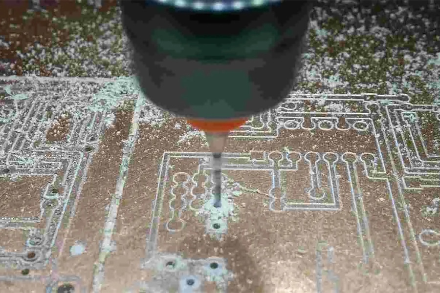
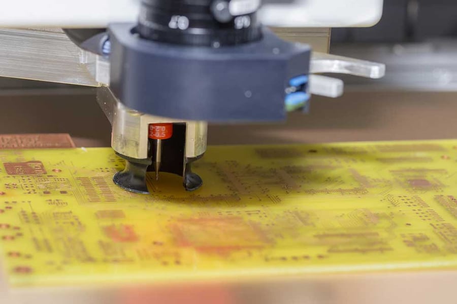
PCB drilling is a crucial step in PCB fabrication, responsible for creating holes that allow components to be mounted and different circuit layers to be connected. This guide will provide PCB designers, engineers, and manufacturers with a comprehensive overview of the entire PCB drilling process.
We will cover everything you need to know about PCB holes – from common hole types like PTH and buried vias to specialized holes like backdrilled vias. You’ll learn about cutting-edge drilling techniques, critical process parameters, quality control standards, and tips for optimizing hole fabrication.
By the end, you’ll have an in-depth understanding of:
- The role and importance of PCB drilling
- modern PCB drilling methods and equipment
- How to set up and carry out the drilling process for quality results
- Types of PCB holes and their design considerations
- Standards for evaluating drilling quality
- Troubleshooting and optimizing the drilling process
Equipped with this practical guide, PCB designers can design manufacturable boards, engineers can oversee production, and fabricators can hone their drilling capabilities. Let’s start unlocking the essentials of PCB drilling!
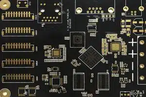
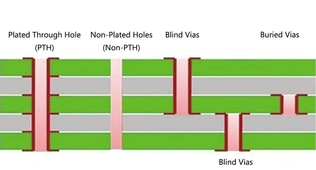
PCB Via Hole Types
PCBs require many precisely placed holes that serve mechanical and electrical functions. While all holes are physically “drilled”, different hole types have unique definitions, fabrication steps, and design considerations. Major categories include:
- Plated Through Holes
PTHs refer to holes that span the entire PCB thickness and have conductive metal plating on the internal walls. This allows components leads to pass through and connect circuits on different layers. PTH dimensions, pad sizes, plating thickness all impact manufacturability. - Non-Plated Through Holes (NPTH)
Unlike PTHs, NPTHs refer to unplated vertical holes in a PCB. They are primarily used for installing mechanical fasteners like screws, spacers, and supportive pins that anchor PCB stack assemblies. Care must be taken to ensure adequate spacing from internal circuitry. - Blind/Buried Vias
Unlike PTHs, blind/buried vias do not span the full PCB thickness. Blind vias stop at an internal layer while buried vias are encapsulated internally. Advanced drilling and layer stacking are required. High-density designs utilize many blind/buried vias. - Micro Vias
Micro vias describe small vias with diameters below 150um used to transit between adjacent layers. Their fabrication requires specialized laser/mechanical drilling to hit tolerances. Micro vias save space and cost versus traditional vias in multilayer boards. - Fastener Holes
Fastener holes provide openings for screws, bolts, and other fastening hardware to mount PCB assemblies to enclosures, stands or other structures. While serving a mechanical function, proper spacing from traces and pads is necessary… - Mounting Holes
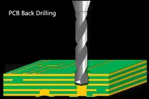
Mounting holes refer to holes reserved for attaching the completed PCB assembly to external mechanical structures. - Backdrilled Holes
Backdrilled Holes refer to a special category of plated through holes that incorporate targeted depth controlled drilling to remove the upper half of the plated barrel after initial full depth drilling. This is done to minimize the risk of unwanted stubs causing impedance discontinuities in high frequency signals through vertical interconnects. Backdrilling thereby enhances circuit performance by smoothening transitions. - Via-in-Pad
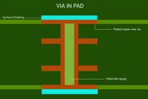
Vias in Pad refers to plated through hole vias that are intentionally designed to overlap with component soldering pads. This allows vertical transitions through vias to be realized underneath mounted components. Additional mechanical alignment integrity is achieved. - Filling Vias
Via filling is a fabrication technique of inserting conductive or non-conductive epoxy material into these vertical interconnecting holes after initial drilling and plating. Epoxy filling can be partial or completely fill up the entire via barrel.
- Half-holes
Plated Half-Holes, also referred to Castellated Holes, are rows of holes drilled alongside the boundaries of a rigid printed circuit board, then to be through plated and milled off half. You may have seen some Wi-fi modules which then soldered onto a larger PCB similar to the way in which ICs are mounted. Plated half-holes are mainly used for board-on-board connections, mostly where two PCB boards with different technologies are soldered together. - Thermal Vias
Thermal Vias are simple plated through holes that located under a surface-mounted heat source component in a PCB board that allows heat transfer. The vias establish a low thermal resistance path from the top copper to the bottom side of the PCB. While, only one via cannot dissipate heat well, and generally requires vias Array.
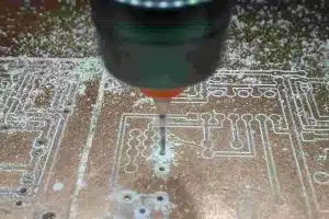
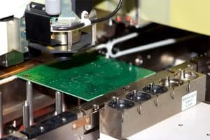
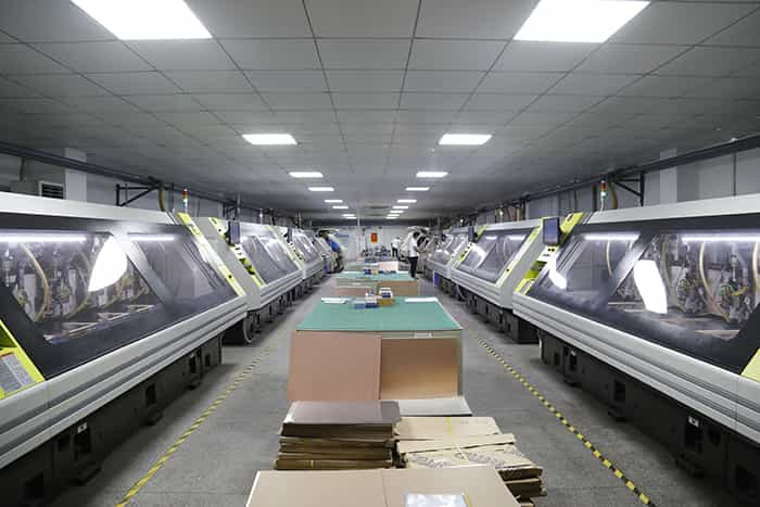
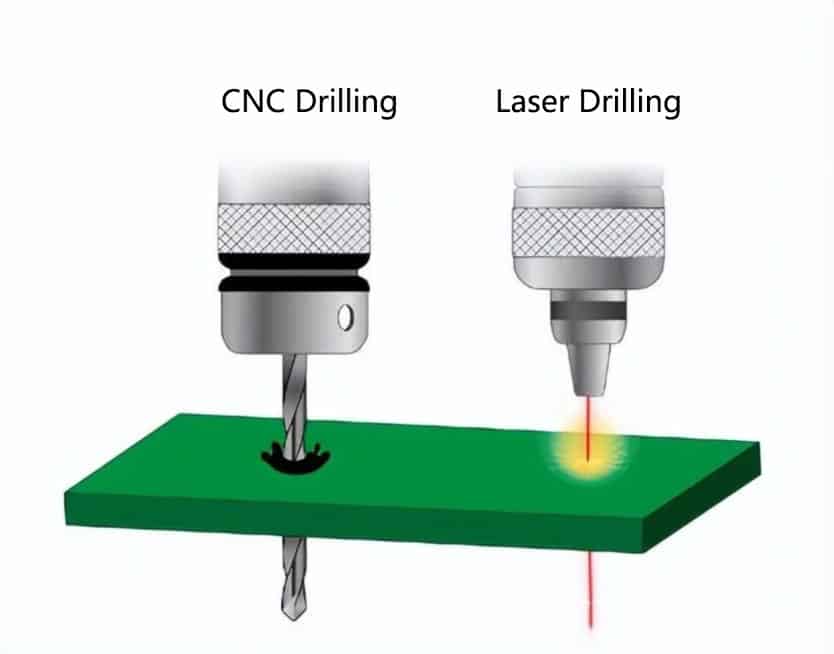
PCB Drilling Methods
While fundamentals are consistent, drilling methodology is an equally vital choice:
Automated Drilling
– High volume production favors automated drilling rigs with programmable direct numerical control.
– Multi-spindle simultaneous operations ensure fastest cycle times and lowest cost per hole.
– Limited in terms of hole size upper limits and material flexibility.
Manual Mechanical Drilling
– Using milling machine beds with adjustable X-Y tables is slower but versatile.
– Caters well to quick-turn prototypes with customizable hole patterns.
– Operator skill influences precision plus risk of human errors.
Laser Drilling
– Extremely small hole diameters down to <50 um possible.
– Minimal mechanical stresses prevent microcracking issues.
– Provides great depth control though slower than mechanical processes.
– Restricted only by line of sight access to target hole location.
Preparation Before PCB Drilling
Thorough preparation is indispensable for achieving target hole quality in terms of accuracy, precision, geometry and hole wall integrity. We focus on three main areas of preparation:
Mechanical rigidity and thermal properties of the PCB substrate directly impact drilling behavior. Popular substrates like FR-4, Rogers, Polyimide have drastically different glass transition temperatures, thermal expansion coefficients, and copper adhesion strengths – all of which guide drill process parameters.
Drilling Drawings and Documentation
Every PCB design has unique layout density, hole dimensions and drill patterns which benefit from custom drill data files. These files guide the sequence of hole drilling, selection of appropriate drill bits based on hole spacing constraints and different technique parameter combinations to balance productivity and drill life.
Equipment and Fixtures
Finally, the capabilities of drilling machines, quality & material properties of drill bits and support tooling influence productivity. Rigid bottom support plates aid perpendicularity while parameters control bit temperature and impregnation.
PCB Board Material Selection
As the drill bit mechanically shears through the laminate, factors like tensile strength, thermal conductivity, and copper foil treatments affect quality:
– Brittle substrates prone to microcracking under drilling stresses. Pre-drill backups prevent crack propagation.
– High Tg materials like polyimide withstand high temperatures. But their poor thermal conductivity concentrates heat – requiring peck drilling.
– Thick copper layers with unfinished foil surfaces wear drill flutes faster. Lubricants aid friction and chip clearance.
Drilling Documentation
Drill data files balance production needs and capabilities based on four main considerations:
– Total Hole Count & Hole Density – Directly impacts tooling requirements and cycle times.
– Hole Size Distribution – Guides optimal stack sequencing with different diameter drill bits.
– Position Accuracy Requirements – Tools and parameters for ±50um vs ±15um tolerances vary greatly.
– Via In Pad Constraints – Determine if secondary reaming steps are necessitated.
Equipment and Tooling Confirms
Suitable equipment and tooling selection hinges on target hole specifications and capabilities:
– Mechanical vs Laser/Etching Drills – Tradeoffs exist for taper control, small diameters, and material compatibility.
– Drill Bit Properties – Needed margins on geometrical & tool-life parameters.
– Support Tooling – Backup plates, parameter guides, vertical stops etc.
PCB Drilling Process Workflow
1. Machine Setup
– Clean drill table; Secure board + backup plate stackup; Install drill bits
– Select suitable drilling parameters – speeds, feeds, peck depths
– Adjust vacuum, coolant pressure, vertical stops
2. Initial First Hole Alignment
– Use optical camera to identify alignment holes or fiducials
– Automatically align spindle to pre-programmed first hole offset location
3. Drilling Sequence Commencement
– Machine starts autonomous drilling of holes in optimized sequence per drill file
– Alternates different diameter drill bits as programmed
– Applies techniques like pecking and dwelling when required
4. Breakthrough Detection
– Modern systems use sudden torque spikes to differentiate breakthrough point
– Retracts drill bit precisely to avoid back side tear-outs
5. Hole Quality Inspection
– Both during and post drilling, holes examined for circularity, barrels, skips
– Automated optical inspection probes measure + verify hole position accuracy
– Cross-sections reveal taper, hole walls and indications of charring
Considerations For Selecting Drills In PCB Drilling
Choosing suitable drill bit dimensions and types is crucial for achieving design intent with the fabrication process. Key selection criteria include:
Drill Diameter
- Match drill sizes to component lead widths
- Maintain adequate annular ring distances for soldering joints
- Account for hole tolerance and drill accuracy variations
- Consider board thickness to avoid drill walking
Minimize Aspect Ratio
- High depth to diameter proportions cause plating and reliability risks
- Target 10:1 ratio for typical through holes as guidance
Leverage Depth Control Of Blind/Buried Vias
- Optimized layer transitions with staggered depths
- Far lower ratios simplify plating throwing power needs
Specialist Micro Drills For Dense Packaging
- Laser drilling extends capabilities below 0.15mm
- Tight process controls realize modern HDI designs
Proactively collaborating with fabrication partners aids drill selection. Plant capabilities, measured tolerance data and depth limitations guide defining appropriate drill sizes.
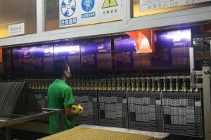
PCB Drilling Quality Control
As an intricate fabrication step, drilling performance directly impacts overall PCB quality and reliability. Stringent quality targets must be maintained through measurements, testing and optimizations:
Drilling Quality Standards
– Hole Diameter Tolerance – +/- 10μm variance allowance common
– Perpendicularity Rating – >89° angle from panel plane
– Hole Circularity – Diameter uniformity circumferentially
– Plating Thickness – 25μm min annular ring on hole walls
Inspection Methods
– CMM Validation – Optical coordinate checker verifies hole positions
– Microscopy – Barreling, smear, hole wall integrity assessed
– Cross-Sectioning – Reveals taper, pad lifting, indications of overheating
Process Tuning & Upgrades
– Parameter Refinement – Peck depth, spindle speeds balanced
– Bit Reconditioning – Flute sharpening or replacements
– Equipment Retrofits – Programmable coolant, pulsed lasers etc.
PCB Drilling Troubleshooting FAQ
Despite best practices, drilling issues manifest requiring rapid solutions:
Q: Smearing and conductive debris in holes?
A: Lower feed rates, prerinsing and anti-smear coatings can mitigate. If severe, desmear processing may still be needed post-drilling.
Q: Bore Taper – Larger exit hole diameters?
A: Insufficient backing support is the primary culprit. A rigid entry/exit plate sandwich upkeeps perpendicularity. Entry ≥ 1.5x exit burr heights.
Q: Out-Of-Position holes beyond tolerances?
A: Thermal instability or worn drill guides are likely causes. Upgrade water-soluble coolants and ensure secure holding fixtures prevent workpiece shifts.
DFM Drill Validation Tips for PCB Designers
During layout, designers must be cognizant of manufacturability constraints related to drilling. Key checks include:
**The aspect ratio must be kept to a minimum to avoid drill wear**
– Higher thickness to hole ratios cause frequent drill breakages. Define stock sizes upfront per layer needs.
**Increase in different drill sizes complicates changeovers**
– More drill tooling required. Restrict counts by combining similar hole sizes under tolerance when possible.
**Validate Drill Integrity Checks**:
– No connections on NPTH holes
– Match drill counts between file and prints
– Correct identification of plated and non-plated holes
– Mouse bite spacings greater than 0.006′′
**Account For Feature Positions**
– Ensure drills and copper features fall within board profile
– Define arc drill locations adequately
**Review Size and Tolerance Choices**
– Narrow down via sizes to meet aspect ratio guidance
– Specify tolerance classes per hole function
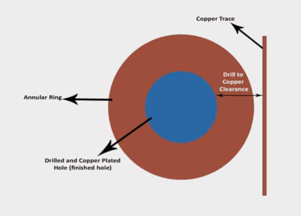
Drill to Copper Clearance
Drill to copper clearance refers to the minimum land spacing mandated between the edge of drilled holes and surrounding copper features like traces, pads or polygons. This clearance safeguards against circuit shorts under drill position deviations.
Typical clearance values are set at 8 mils or above. This ought to exceed the sum of target annular ring width post plating and solder mask web tolerances. Insufficient clearance risks reliability failures from solder wicking or stress cracks across inadequate webs.
So in summary,
Minimum Drill to Copper Clearance = Annular Ring Width + Solder Mask Web Clearance
Both parameters here depend on hole size and plant capabilities. But often 10-12 mil clearances are prudent starting points. If plant feedback indicates positional variations however, clearance budgets must be reassessed accordingly.
Aspect Ratio Considerations
The aspect ratio (AR) refers to the proportional relationship between the depth of a drilled hole relative to its diameter. This ratio critically governs reliable metallization and plating capabilities inside holes, especially for vias interconnects between layers.
The aspect ratio is calculated using the formula:
Aspect Ratio = Depth of Hole / Diameter of Hole
High aspect ratio holes with smaller diameters and deeper depths put greater stress on plating bath throwing power, copper deposition coverage consistency and increase chances of reliability issues over product life cycles.
As a rule of thumb for robust manufacturing, target aspect ratios are:
- 10:1 for typical through-hole vias
- Up to 15:1 for HDI technologies with thinnest dielectrics
- 0.75:1 maintained for microvias
For a common 60 mil thick PCB, minimum drill sizes in the range of 6 to 8 mils are recommended based on hole depth. And greater allowances apply for thicker boards above 93 mils.
Conclusion
We have comprehensively covered PCB drilling essentials spanning hole types, process planning, techniques, quality control and troubleshooting measures.
As intricate as drilling workflows may seem, adhering to design for manufacturability guidelines coupled with collaboration between designers and fabrication partners right from the substrate stages goes a long way.
Technology improvements on advanced drill bits, optimized parameters and inspection systems also continue to shape precision and capabilities.
To learn more about optimizing the drilling process for your next PCB project or resolving current drilling issues, reach out to our engineering experts. Our team brings decades of experience fine-tuning drill operations and infrastructure for Leading PCB manufacturing clients.
We are eager to partner in your PCB drilling journey right from conceptual layout reviews to custom drill file setups all the way through to hole quality verification guidance.
Contact us via email or book a consultation call now to discuss your requirements! Our insights can deliver immense value no matter the production volume or hole intricacy needs.
Related Posts