Table of Contents
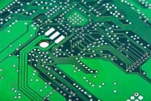
What is Via-in-Pad Technology for PCBs?
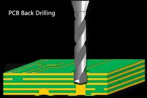
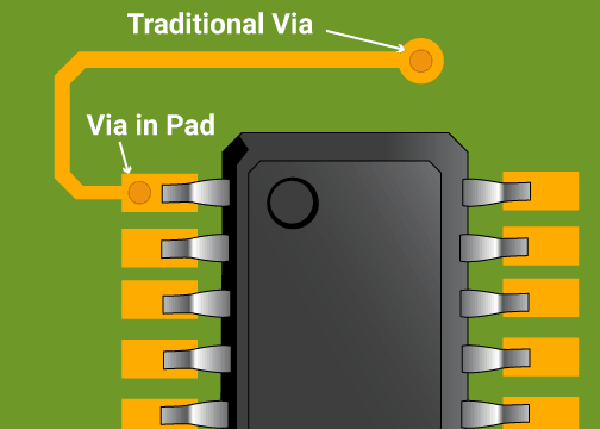
Before jumping into the via-in-pad definition, let’s recap common PCB via types. Plated-through holes (PTHs) are basic vias that span an entire PCB to interconnect layers. Blind and buried vias partially span layers, while microvias (~0.1mm) interconnect adjacent layers. All share a purpose of routing between layers.
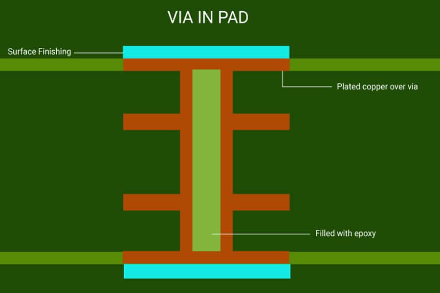
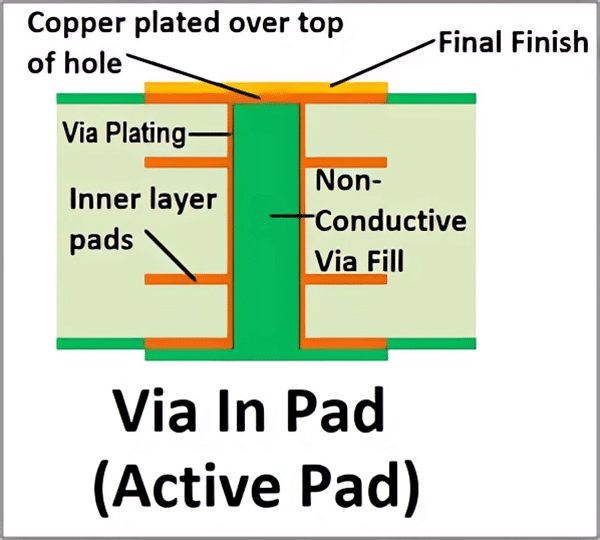
Via-in-pad represents an evolution in PCB design – it places a via structure directly within a surface mount land pad. IPC defines several classes depending on structure specifics, but the key benefit is conserved space. By overlaying elements, via-in-pad effectively eliminates need to route traces between conventional pad and discrete via. This facilitates greater component density and more efficient layouts overall.
As an experienced manufacturer of high-quality PCBs, JHYPCB has refined expertise to fabricate innovative boards using via-in-pad technology reliably. We have qualified process capabilities covering all associated activities like drilling, plating, tinning and solder mask definition. Customers regularly turn to us for advanced solutions that save layers and simplify circuits through integration.
Let’s dive deeper into why PCB designers specify via-in-pad, implementation concerns, reliability factors, and suitable applications that maximize utility. Data shows properly-designed configurations withstand thermal cycling essentially equivalent to pads without vias. By following suitable DFM guidelines, engineers access the considerable benefits while mitigating negative technical risks.
Maximizing Space and Routing Efficiency
The foremost incentive for deploying via-in-pad stems from enlarging PCB utilization efficiency. By consolidating the land pad and interconnecting via into a shared zone, additional space is liberated rather than demanding enlarged surface area to accommodate discrete versions of both. This facilitates several advantages:
- Higher component density: With the footprint consumed by an isolated pad/via combo reduced essentially by half in select instances, packing more elements within the same PCB envelope becomes possible. This enables smaller product designs or allocation of space for more features.
- Layer reduction: When utilizing blind/buried vias originally intended to bridge inner layers, substituting via-in-pad merges connectivity so fewer laminations are necessary in the first place. Complex designs might shed 2-4 layers resulting in lower costs.
- Routing improvement: Space savings translate into up to 30% enhanced routing channels across layers, as traces can navigate more directly without dodging around land pads or blocked zones. Analog designs see lower noise and interference pickup due to shorter unshielded traces possible.
- Cost savings: In addition to fabricated PCB pricing declines from reducing layer counts, via-in-pad also economizes by deleting steps over isolated pads and vias – including separate drilling cycles. Greater component consolidation further lessens expenses additive for BOMs and assembly down the line.
So in environments where high-density population drives innovation like wearables, Internet of Things (IoT) devices, and vehicle electronics, PCB developers leverage via-in-pad to push boundaries. By merging structures intelligently, electrical functionality need not be compromised.
Obstacles to Address with Via-in-Pad
Although the inherent efficiency of combining pad and via is appealing, engineers must account for some challenges at initial design phases to ensure reliability over product lifetimes. These encompass fabrication factors along with operating stresses encountered as boards age:
- Solder wicking: Perhaps most notorious, wayward solder can invade the internal via barrel during reflow, causing electrical shorts or compromising mechanical shear strength where leads attach. Appropriate solder masking is thus vital.
- Reduced soldering heat: The metallic pad/via thermal mass absorbs more heat, slowing reflow. Adjusting profiles to reach adequate temperatures without overshoot is imperative.
- Limitations on rework: If bottom-terminated vias require remediating errant solder joints, less access and visibility complicates heating or solder wick procedures. Rework on via-in-pad may simply be impractical.
- Drilling accuracy: Since vias align flush with pad perimeters without tolerance, CNC drill bit centering mandates precision within 0.1mm often. This assures adequate annular rings prevent masking breaches.
- Thermal cycling strains: Differing expansion rates across copper, laminate materials, and solders coupled with concentrated interfaces heighten stresses that may crack interfaces over operating lifetimes without appropriate design foresight.
By partnering with an experienced manufacturer like JHYPCB possessing robust qualification procedures covering thermal shock testing, inspection, and imaging, engineers can validate entire process chains required to perfect via-in-pad implementations resistant to such mechanisms. Our expertise has refined the necessary DFM particulars like minimum annular rings, thermal reliefs, mask opening tolerances, etc. to actualize durability.
Via-in-Pad Design Guidelines
To counteract the potential pitfalls of adopting via-in-pad technology while harnessing the density and efficiency gains, engineers should adhere to guidelines curated through IPC standards analysis and practical learning:
- Solder mask sizing: Defining openings between 0.2-0.3mm larger than the via pad diameter helps provide adequate insulation against wicking while limiting added space demands. This balances solder flow and electrical isolation.
- Plating: Immersion silver or nickel barrier finishes deter solder leaching into vias better than basic tin surfaces. However, some SMT pads may still utilize solder plating for ideal interconnectivity.
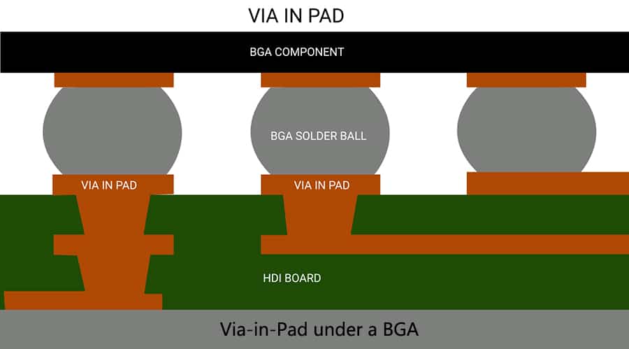
- Pad and via dimensions: Smaller vias down to 0.15mm match well with 0201 chip components, but larger BGA pads and vias from 0.3 to 0.5mm endure mechanical stresses superiorly.
- Tenting vias: Alternatively, solder masking the via bottom aids insulation and reduces wicking risks, but makes rework nearly impossible. Assess based on other reliability factors.
- Thermal relief spokes: Radial copper spokes emanating from the via pad corners help dispel damaging heat concentrations during reflow while retaining superior electrical connectivity vital across DFN pads.
- Test coupon analysis: Rigorous trial assessments through intense temperature cycling, liquid submersion, and destructive shear evaluations best validate minimum tolerances and achieving sturdy solder bonds on via-in-pad specimens.
By partnering with JHYPCB early during concept stages as we have years of experiential data to share, engineers can craft optimized PCB layouts for approving and releasing efficient production runs with minimal revisions. Our time-tested design for manufacturability knowledge supports tackling the challenges of via-in-pad head-on.
Qualifying Robust Via-in-Pad Reliability
To promote widespread industrial acceptance of via-in-pad technology balancing densification with durability, updated standards now furnish definitive inspection criteria and testing procedures for validating acceptable fabrication. These aim to accelerate continual PCB evolution meeting sophisticated functionality demands within highly confined electronics envelopes across markets spanning defense, aerospace, mobile computing, automotive, medical, and more.
Among the foremost references lies IPC-6012D: “Qualification and Performance Specification for Rigid Printed Circuit Boards” which delineates testing protocols across:
- Thermal stress cycling – Typically enduring 100 cycles spanning -55°C to 125°C, well-designed via-in-pad should exhibit no discernible cracked joints or electrical malfunctions.
- Mechanical shock/vibration – Up to 1500G loads across 3 axes affirms robust adhesion.
- Liquid exposure – Immersing powered boards in solutions of water, chemicals or other potential contaminants checks insulation barriers.
- Microsectioning – Metallurgical cross-sections must reveal quality plated barrels without excessive voids.
- X-ray inspection – Confirms drill centering, mask openings, annular ring dimensions, and pads bonds meet specification.
At JHYPCB, we incorporate these test regimens among our rigorous quality assurance practices when customers request via-in-pad on delivered PCBs to completely satisfy industry performance mandates. Please inquire with our engineering team to leverage material expertise as you qualify innovative board layouts making the most of via-in-pad capabilities! We also continually validate manufacturing enhancements ensuring these standards are exceeded.
Ideal Applications for Via-in-Pad
Given the design considerations required to fully leverage benefits of via-in-pad without compromising long-term reliability, certain PCB implementations stand to gain most from committing to this technology. These encompass situations where:
- Extreme space constraints demand maximum component packing density – Wearables, smartphones, and microcontrollers all require very efficient utilization.
- Lower layer counts simplify fabrication for budget sensitivity – Consumer electronics often value cost savings.
- Mostly SMT parts are populated – Especially fine-pitch ICs where rework is improbable anyway.
- Short production runs limit reliability risks – If cycling lifetime is scoped in months not years.
- Analog signal integrity is paramount – Shorter unrouted trace spans reduce interference.
Conversely, designs handling higher power transmissions or larger mechanical loads may continue favoring more conventional discrete pads and vias over integrated configurations, as heat dissipation demands or potential rework still outweigh density incentives. This underscores thoroughly assessing end-use operating conditions before modernizing legacy layouts.
With competency delivering over 500 PCB varieties annually featuring HDI technology like via-in-pad among other techniques boosting functionality, the application engineers at JHYPCB can guide appropriate selection tailored to your specific project constraints. Consult us to determine whether migrating to via-in-pad promotes your core objectives. We help extract every efficiency advancement accessible through informed adoption that mitigates risk factors.
Realizing Next-Generation PCB Innovation
As consumer appetite for more features squeezed into smaller mobile products accelerates, PCB developers face intensifying demands on squeezing greater functionality into less space. This drives migration to sophisticated design paradigms and fabrication processes that depart from conventional techniques reaching their limits.
Via-in-pad construction represents one such high-density strategy gaining traction as designers pursue routing efficiency and component consolidation. By assimilating the land pad and interconnecting via into a shared footprint, boards save layers and space that would otherwise demand expansion. decades ago. This supports improved analog performance, lower production costs, and shorter design cycles.
However, smooth implementation also weighs several reliability factors from potential solder wicking and rework limitations to material stresses that may compromise integrity over product lifetimes. This requires careful design foresight and experience with the nuances of HDI processing. As such, partnering with an advanced manufacturer like JHYPCB helps expedite adopting via-in-pad technology safely.
Our holistic expertise in this arena spanning fabrication through inspection ensures you actualize miniaturization goals without jeopardizing durability. We invite you to explore how integrating via-in-pad into upcoming PCB layout revisions may solve struggles reached by status quo solutions. Discover faster times to market with designs on the leading edge!