Blind Vias, Buried Vias in PCBs – A Complete Guide
Home » Blind Vias, Buried Vias in PCBs – A Complete Guide
Blind vias and buried vias enable improved signal routing, component density, performance, and simplified PCB stackups essential for complex, high-speed designs. This article explains what blind and buried vias are and key considerations for implementation.
Table of Contents
Introduction
As printed circuit boards continue to become more complex and highly integrated, newer via structures have been developed to facilitate the complex routing and layering demands. In previous articles, we explored common via types like plated-through holes (PTHs), non-plated through holes, and microvias. However, the constraints of traditional straight thru-hole via structures often lead designers to utilize blind vias and buried vias in complex multilayer PCB boards. This allows them to optimize performance, density, and manufacturing cost requirements.
Blind vias and buried vias serve unique purposes that allow PCB designers flexibility in stacking and connecting layers. Understanding the key differences between the two is imperative for both designers and PCB manufacturers alike when developing high-speed, high-density boards. In this article, we’ll define blind vias and buried vias and discuss their advantages, layout considerations, and applications across industries.
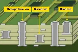
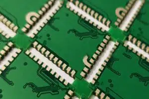
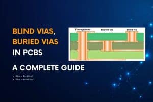
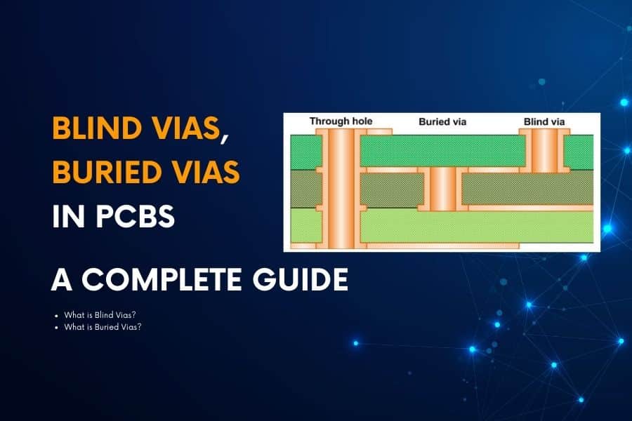
Via Types in PCB Board
What Are Blind Vias?
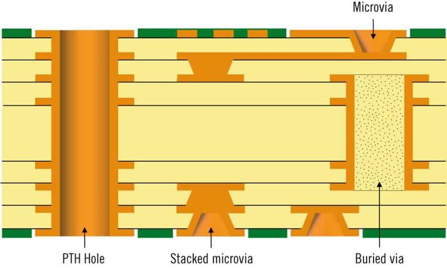
Blind vias are holes that provide an electrical connection between an inner layer and an outer layer of a multilayer printed circuit board without passing through the entire PCB stackup. In other words, blind vias connect an embedded inner layer to only one of the outer layers, terminating before reaching the opposite side. They are “blind” because they do not pass completely through the circuit board.
Some key characteristics of blind vias:
Connect an internal layer and just one external layer
Stop before reaching the opposite outer surface
The non-connected outer layer is left intact – the blind via does not penetrate it
Often used in higher layer-count PCBs (>4 layers)
Typically smaller diameters than through-hole vias
Requires very accurate alignment and drilling
The major benefits offered by using blind vias include:
Higher component density: By not penetrating the entire PCB layer stack, blind vias occupy less space compared to regular plated thru-holes, allowing components to be placed more densely. Component density improvements of 15-20% can be achieved.
Flexible routing: Blind vias allow connections between inner and outer layers providing more routing options, especially in dense, complex designs.
Lower costs: They require fewer lamination layers compared to using regular PTHs or even buried vias. The simpler layer stack lowers materials and processing costs.
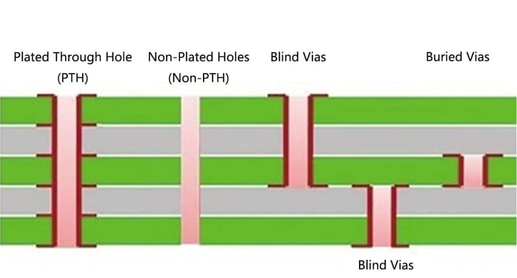
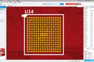
PTH, Non-PTH, Blind Vias, and Buried Vias
What Are Buried Vias?
Buried vias are plated-through holes that provide connections between two or more internal layers of a multilayer PCB without connecting to either outer layer. They are considered “buried” because they are embedded inside the board, with conductive layers above and below them.
Key characteristics of buried vias:
Connect two or more adjacent inner layers
Do not connect to either of the outer layers
Require precise alignment between layers
Well-suited for higher density interconnects
Difficult to inspect visually or test physically
There are several advantages to utilizing buried vias:
Reduced layer count: By skipping outer layers, buried vias allow designers to utilize fewer lamination layers to route between inner layers. This can greatly simplify designs.
Signal integrity: Buried vias provide short and straight paths for signals between inner layers, leading to better signal integrity compared to indirect routes.
Lower capacitance: Lack of connection to external layers means buried vias provide less parasitic capacitance. This helps high frequency performance.
Shielding: They avoid interfering signals on outer board layers that may couple to inner traces. This shields and contained signals.
Differences Between Blind Vias and Buried Vias
While blind vias and buried vias serve unique connectivity roles, differentiating when and where to implement one over the other is important in complex PCBs. Keeping their contrasts and tradeoffs clear ensures the appropriate choice during design.
Key differences include:
Connectivity:
Blind vias – Connect an inner layer to ONE outer layer
Buried vias – Connect two or more inner layers only
Penetration:
Blind vias – Partially penetrate the PCB stackup
Buried vias – Fully penetrate the layers they interconnect
Inspection:
Blind vias – One opening allows visual and physical test access
Buried vias – No visual access or physical probe test points
Manufacturing:
Blind vias – Require precise depth control to stop at correct layer
Buried vias – Require extremely tight registration between layers
Reliability concerns such as moisture ingress or delamination faults differ between blind and buried vias too. Designers must consider all these nuanced factors when applying them. A strong partnership with your PCB manufacturer is essential to leverage them appropriately.
Considerations for Using Blind and Buried Vias
While blind vias and buried vias enable smaller, higher performance PCBs, they also impose some design and fabrication rules that must be followed. Understanding limitations and best practices for implementation is key to maximizing benefits. Some key considerations include:
Manufacturing Capabilities
Ensure your PCB partner’s process supports needed layer counts and via sizes
Tighter registration tolerances are required (±0.002” or less)
Additional lamination, drilling, and plating steps add cost
Testing and Inspection
Visual inspection and physical probing is restricted
X-ray imaging or specialized microscopy usually required
Impedance, resistance, and continuity testing is essential
Reliability Factors
Thermal expansion and moisture swelling stresses require analysis
Interface separation or cracked connections may develop
Redundant vias and testing helps safeguard buried connections
Design Rules
Limit use to 6-8 layers to control yield and cost tradeoffs
Save weight through higher component packaging densities
Portable/Wearable Consumer Goods
Interconnect stacked components without increasing footprint area
Achieve product miniaturization goals
In almost every instance, blind and buried vias enable improved routing density, component packaging, electrical performance, and reliability essential to modern electronic products spanning commercial to military applications. When designed properly, they are a critical PCB fabrication tool for solving shrinking, higher performance demands.
Conclusion
As PCBs continue getting more complex across a wide range of products and industries, leveraging the right via structures is imperative. Blind vias and buried vias each serve unique connectivity roles for routing signals between layers. Understanding when to implement blind vias to link inner and outer layers versus buried vias between two inner layers allows designers optimization flexibility.
Blind vias and buried vias also enable improved component density, simpler layer stackups, superior high-speed signal integrity, and reduced costs compared to traditional PTHs. However, designers must weigh manufacturability and reliability considerations when applying them. Having an experienced PCB manufacturer as a partner ensures you follow proven design rules and achieve yield targets.
At JHYPCB, we have extensive expertise producing PCBs with blind vias and buried vias per your custom specifications. Our advanced process capabilities guarantee quality and reliability for your most demanding electronics designs. Contact us today to discuss how blind vias and buried vias can provide an ideal, cost-effective interconnect solution for your next product.
JHYPCB is a leading PCB prototyping, PCB manufacturing and assembly service provider in China, offering quick turn PCB prototyping, multi-layer PCB manufacturing and turnkey PCB assembly services.