Identifying and Processing Via-In-Pad in PCB Design
Home » Identifying and Processing Via-In-Pad in PCB Design
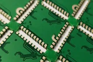
Via-in-pad refers to drilling vias on pads, commonly used for high density SMD and BGA pads. This article covers in detail the design guidelines, manufacturing process of via-in-pad, and makes comparison of with and without via-in-pad process.
Via-in-pad refers to vias drilled on pads. The pads are usually SMD pads sized 0603 or larger and BGA pads. They are commonly known as VIP (via in pad). The vias on through-hole component pads are not considered as via-in-pad since those vias are needed for inserting and soldering the component leads.
With the trend of electronic products becoming lighter, thinner and smaller, PCBs are also evolving towards higher density and complexity. As a result, electronic components are getting smaller in size as well. For instance, BGA components have smaller package size and smaller pin pitch. The routing space between BGA pins can be very limited, requiring vias for layer transition in routing.
When the BGA pin pitch is too small for fan-out routing, drilling vias in pads is the only solution. Another scenario is when bypass capacitors are placed on the back side of a BGA component with dense pins so that it’s impossible to route vias without hitting any pads, drilling vias in capacitor pads becomes necessary. Therefore, two types of via-in-pad exist: on BGA pads and on SMD pads.
It is recommended to avoid via-in-pad design when routing space allows. Manufacturing cost for boards with via-in-pad is usually very high and cycle time much longer.
Design Guidelines for Via-In-Pad
No Need for Via-In-Pad
Fan-out routing should be performed before any layers routing. For BGA fan-out, vias need to be centered between BGA pads if the pin count is high while routing space is limited. Typical fan-out parameters for BGA: via diameter 0.15-0.2mm, trace width 3-4mil, annular ring 0.3-0.4mm. So the minimum BGA pin pitch for fan-out routing is 0.35mm.
Via-In-Pad Necessary
Before BGA fan-out, check the via hole size. Otherwise improper via size fails the fan-out or generates incorrect result. Design via-in-pad when BGA pin pitch is too small for fan-out. Route BGA pins thru other layers or from component side.
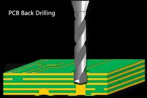
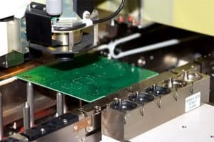
Manufacturing Process for Via-In-Pad
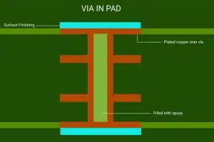
Vias on BGA pads are generally considered as via-in-pad. These vias need to be plugged and plated to facilitate soldering, unless otherwise specified by customers.
For boards with fully plugged vias per customer request, vias on any SMD pads are also treated as via-in-pad.
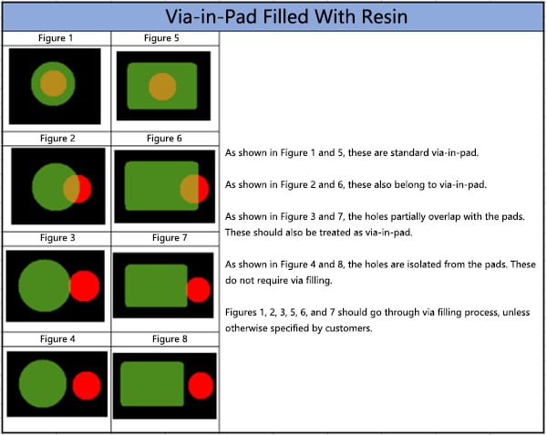
Via-in-Pad Filled with Resin and manufacturing process
Explanation of Via-In-Pad
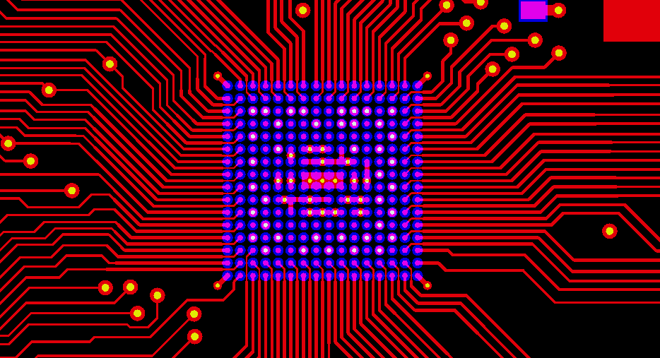
01. Via-in-pad on BGA
Most components do not need via-in-pad design due to less pins. For BGA components, fan-out vias take up routing space. Design these vias as via-in-pad, centered on BGA pad, can create routing channels. When pin pitch is too small for routing, use other layers thru via-in-pad.
Via-in-pad on BGA
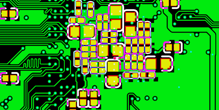
02. Via-in-pad for bypass capacitor
Lots of vias are needed when routing BGA pins on inner layers. It becomes very difficult to route bypass capacitors on BGA back side without hitting any vias. Therefore these vias are designed as via-in-pad on capacitor pads.
Via-in-pad for bypass capacitor
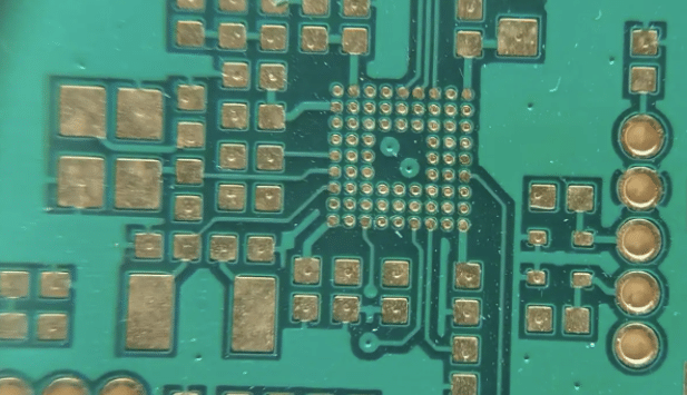
03. Without via-in-pad process
For boards designed with via-in-pad but did not go thru via plugging process, poor solder joint strength, voids inside drilled holes, solder balls under pads could occur due to limited soldering area.
Without via-in-pad process
04. With via-in-pad process
BGA pad size is small itself. Adding a via-in-pad further reduces the soldering area significantly. Plugging and plating the via-in-pad to planarize hole wall facilitates soldering and avoids the issues mentioned above.
With via-in-pad process
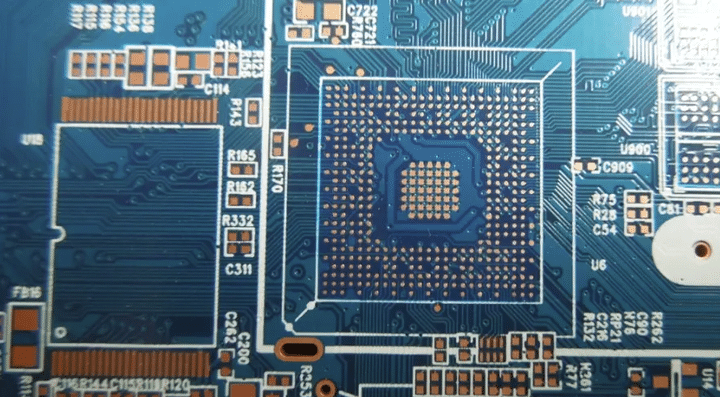
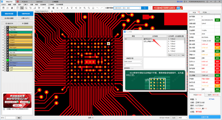
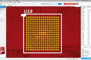
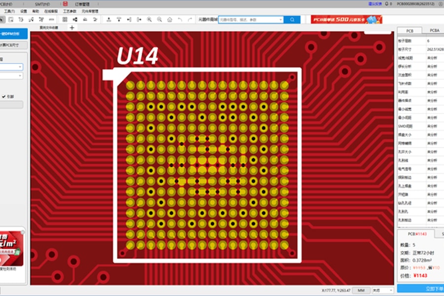
Huaqiu DFM Checks Via-in-Pad
DFM Checks Via-in-Pad
Huaqiu DFM analyzes design files with one click to detect any via-in-pad, and provides suggestions to engineers on modifying the via-in-pad to reduce cost. It also reminds PCB manufacturers the via plugging process is required for boards with via-in-pad designed.
DFM Checks Via-in-Pad
Huaqiu DFM is an independently developed PCB design for manufacturability analysis software by Huachuang Electronic. Offered free of charge, its key functions include: bare board analysis, PCBA analysis, optimization recommendations, cost & lead time estimates, supply chain orders, impedance calculations, etc. Targeting at identifying all potential quality issues ahead of manufacturing to reduce iterations and cost while enhancing product competitiveness.
JHYPCB is a leading PCB prototyping, PCB manufacturing and assembly service provider in China, offering quick turn PCB prototyping, multi-layer PCB manufacturing and turnkey PCB assembly services.