Understanding Plated Through Holes (PTH) for Printed Circuit Boards
Home » Understanding Plated Through Holes (PTH) for Printed Circuit Boards
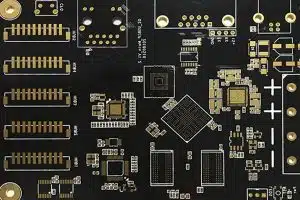
Plated through holes (PTHs) are vital in printed circuit boards for enabling reliable connectivity between layers. This article explores PTHs in depth—from their key benefits like durable interlayer connections and flexible component placement, to critical design considerations around hole size, spacing, depth. We also contrast PTHs to cheaper non-plated holes, and overview popular alternatives like blind and buried vias and their ideal use cases. For PCB designers and manufacturers, our insights help inform effective PTH integration tailored to your product requirements. Reach out to explore our professional PCB fabrication utilizing PTHs.
Introduction
Printed circuit boards play a vital role in electronics by providing the foundation for mounting and connecting electronic components. To facilitate these electrical connections, PCBs utilize holes that are plated with conductive metals—called plated through holes (PTHs).
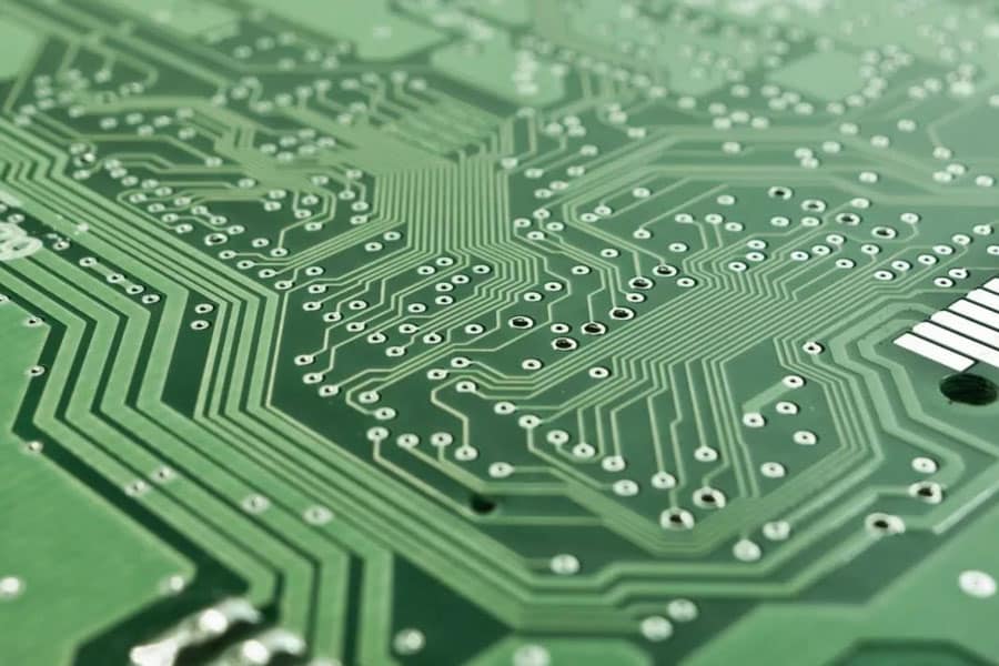
PTHs are hole reinforcements that allow connections of traces and components from one side of the board to the other. The interior walls of these holes are plated with highly conductive metals such as copper, gold, or silver, creating a continuous lining that enables signals to pass between PCB layers.
This interconnectivity makes PTHs invaluable for multilayer boards housing complex circuits. By providing reliable interlayer connections, PTHs grant greater layout flexibility for designers to position critical traces and components.
In this article, we’ll cover PTHs in depth—from their key benefits to critical design considerations. We’ll also contrast them with non-plated holes and other popular hole types like blind and buried vias. Our insights are geared to aid PCB designers and manufacturers in leveraging PTHs effectively.
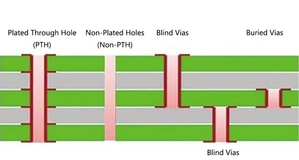
PCB Via Types
Table of Contents
Main Benefits of Using PTHs
Reliable Interlayer Connections
The key benefit PTHs provide is reliable connectivity between layers in multilayer PCBs. As holes pass through the entire board, their plated walls form a continuous metal barrel connecting traces across layers. This allows signals to travel between layers with continuity.
The conductive plating essentially “wires” a connection through the length of a PTH. Typical platings like copper or gold provide excellent conductivity while resisting corrosion—enabling PTHs to maintain high signal integrity across layers.
Component and Trace Positions on Both Sides
PTHs also enable placement of components and routing of traces on both sides of a PCB. With connections bridging both layers, components can be mounted and traces routed above or below a board.
This facilitates optimized component placement for compact layouts and complex routing paths for multilayer circuits; expanding design freedom and efficiency. Components need not compete for space on one side when both surfaces can be utilized.
Superior Reliability vs Non-Plated Holes
The continuous plating along hole walls also makes PTHs far more reliable than non-plated through holes. In non-plated holes, signal travel depends on the alignment/contact between conductive elements inserted in the hole on each layer. This contact wears with vibration, heat cycling etc., progressively introducing resistance.
PTH plating eliminates this dependence on contact alignment inside the hole—greatly boosting connection durability and consistency across temperature or vibration changes.
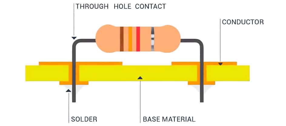
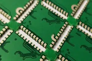
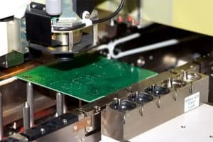
The components are mounted on the PCB board by inserting their leads through the respective hole
In through-hole technology, the components are mounted on the PCB board by inserting their leads through the respective hole. These holes are called through holes since they are drilled from the top to the bottom of the board.
PTH Design Considerations
Hole Size and Components
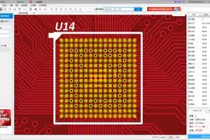
A primary PTH design consideration is sizing holes appropriately to accommodate component leads or attachments passing through them. Holes must match the lead diameter to enable flush connections.
If holes are too small, leads cannot insert through. If overly large, connection reliability weakens and more substrate material is consumed unnecessarily during drilling. As most hole sizes fall between 0.3-0.8mm, precise drilling tools are essential.
Hole Placement and Routing
Strategic hole placement is also key for facilitating simpler routing. Holes should align as near as possible to the intended path of routing traces, minimizing the lengths traces must run before reaching the PTH connections.
Similar considerations apply for component hole alignments. Optimal placement has holes intersecting component solder points—preventing traces taking indirect paths between attachments and hole connections.
Hole Spacing
Sufficient spacing between PTHs is vital to prevent copper plating merger between adjacent holes. As a rule, hole spacing should be no less than 2 times their finished diameter post-plating. This prevents shorting while conserving drilling resources.
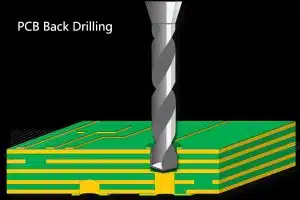
Deeper Holes Cost More
Finally, depth impacts costs. As holes drill through more layers, drill bit wear, material waste, and plating difficulty increases. Shallower PTHs that serve a common subset of layers often suffice over full-depth holes between all layers.
Comparing PTHs and Non-Plated Holes
While plated through holes are the premium option for interlayer connectivity, non-plated holes present a simpler and cheaper alternative for less demanding applications. Here we contrast the two approaches:
Cost and Process Comparison
The key distinction lies in the plating process. Non-plated holes skip this step—saving production time and costs compared to PTHs. Without plating however, reliability suffers from the lack of physical contact between conductive elements inserted into the holes on each layer.
Reliability and Consistency
For products facing vibration, shock, or fluctuating temperatures, non-plated holes carry substantial risks as metal expansion/contraction can disturb the element alignment inside holes over time. This progressively introduces resistance or intermittent faults.
PTHs mitigate this through consistent plating bonding traces regardless of environmental conditions or mechanical stress. The superior reliability and signal integrity justify their use for mission-critical electronics.
Recommendations on Selecting Hole Type
For simple, single-sided PCB boards not requiring interlayer connections, non-plated holes present an affordable option. However, multilayer boards with components mounted on both sides often demand PTH’s durable connectivity. High frequency or safety critical systems also necessitate the assurance of plated holes.
Assessing signal integrity, reliability requirements, and product lifespan expectations helps identify ideal hole selection early in the design process.
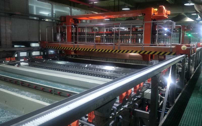
Plated Through Hole Process
Other Plated Hole Types
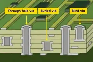
While PTHs allow connectivity across the full length of a PCB, other plated hole types enable reliable connections through partial subsets of layers. Two common varieties are:
Blind Vias: These are holes plated through a few sequential layers but do not pass fully through the entire board. Blind vias connect an intermediate layer to only one external side of a PCB.
They conserve material compared to full PTHs when connections only service a mid-layer region like connecting surface mount chips to internal signal layers beneath.
Buried Vias: In contrast to blind vias reaching one side, buried vias connect two or more inner layers without connecting externally at all. They link internal node “islands”, allowing complex routing architectures splitting the board into functional blocks.
By relegating connections within layer subsets, both blind and buried vias optimize connection density versus full PTHs. They also reduce costs when high interlayer connectivity concentrates within specific regions.
As plated holes, both varieties share PTH design considerations like sizing, spacing, and plating to ensure reliable layer-to-layer connections when needed.
Conclusion
In summary, plated through holes serve an invaluable role in printed circuit boards by enabling durable connectivity of traces, pads, and components across all layers. Their conductive plating facilitates unimpeded signal travel through the length of a multilayer board regardless of mechanical or thermal conditions.
While non-plated holes provide a cheaper alternative, PTHs’ reliability and robustness justify their prominence in mission-critical, high-frequency, and environmentally challenged electronics. Their careful integration early in the design process through mindful considerations around size, spacing, depth, and layout optimizations can make or break a board’s overall performance.
As a full-service PCB manufacturer catering to prototypes through production volumes, JHYPCB has extensive expertise in producing boards leveraging PTHs. If you have a new application demanding high interconnectivity across layers, please reach out to discuss your requirements. Our engineers can provide guidance to harness PTHs while meeting budget needs effectively.
We hope this piece provided useful foundations around plated-through holes and how to leverage them best when designing your next board!
JHYPCB is a leading PCB prototyping, PCB manufacturing and assembly service provider in China, offering quick turn PCB prototyping, multi-layer PCB manufacturing and turnkey PCB assembly services.