sales@pcbjhy.com

Sales Manager: Ms. Megan

+86-13825274100

24/7 Customer Support

+86-13825274100

WeChat and WhatsApp

Leveraging Filled and Capped Vias for Enhanced PCB Reliability

Filled and capped vias are advanced PCB design techniques that measurably enhance connection reliability. Learn when and why to leverage precision via filling and durable capping to prevent moisture ingress, fractures, and short circuits.
Filled and Capped Vias in PCB Design

Table of Contents

Introduction

As PCBs become more complex with higher component densities and more demanding performance requirements, the reliability of plated through holes, micro vias, blind vias and buried vias, and other via structures is increasingly critical. Tiny cracks, moisture ingress, or material fractures in vias can lead to system failures and costly repairs down the road.

This is why leading PCB manufacturers like JHYPCB are utilizing advanced via protection methods such as filled and capped vias more than ever before. When properly implemented, filling and capping vias can strengthen connections, prevent oxidation or outgassing, and enable boards to withstand vibration, mechanical shocks, and extreme temperatures.

In this article, we’ll define what filled and capped vias are, when they should be used, and the measurable reliability improvements you can expect by working with a capable PCB partner to incorporate these enhancements. We’ll also overview JHYPCB’s capabilities and experience delivering high-quality boards with protected vias for everything from consumer devices to industrial equipment to aerospace applications.

As you continue reading, you’ll learn:

  • The differences between filled and capped vias and how they uniquely improve reliability
  • The precise materials used by JHYPCB when filling or capping vias
  • Use cases and applications where filled/capped vias provide the greatest benefits
  • How filled and capped vias enable complex, high-density PCB designs
Various PCB through-hole diagrams

Filled Vias Protect Against Failures

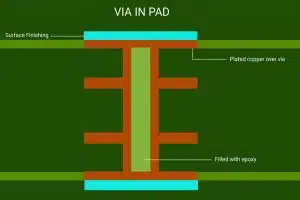
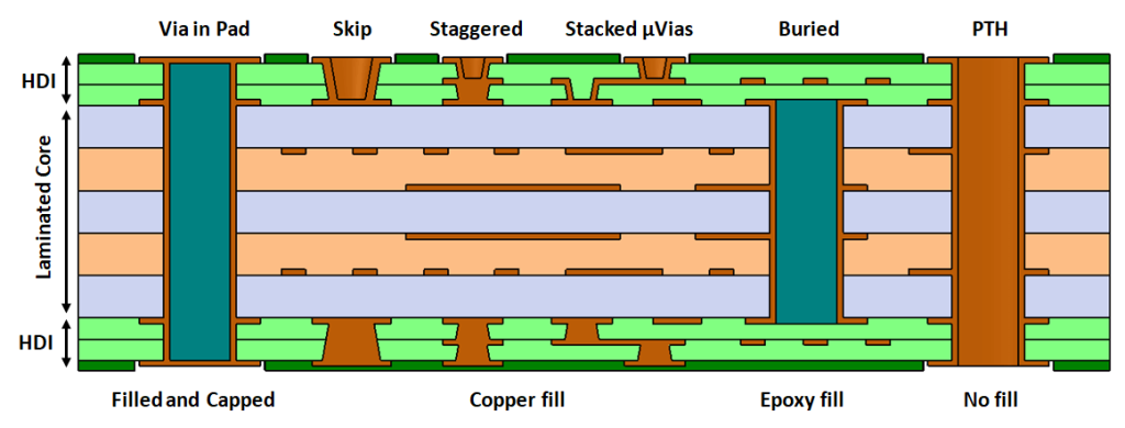
Filled vias are plated through holes, microvias, or other via connections that have been internally filled with a specialized material after drilling and metallization occurs. This extra step enhances reliability by protecting the vital via connection from environmental threats.

As shown in Figure 1 below, filling the remaining space inside a via can prevent oxidation, moisture ingress, outgassing, and other risks that lead to conductivity issues or fractures over time. Common filling materials include epoxies, polymers, and other nonconductive substances that cure solidly inside the barrel of the hole.

Cross-Section of Filled Via

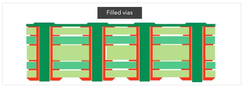
Figure 1: Diagram of a Filled Via (Source: JHYPCB)

Precision matters greatly when implementing filled vias. The right fill ratio is vital — too much material can cause issues, while too little leaves the via insufficiently protected. This is why choosing an experienced PCB manufacturer is recommended. For example, JHYPCB utilizes advanced processes to control flow rate, temperature, and fill cure times to optimize reliability.

The applications where filled vias make the most impact include:

  • High frequency circuits susceptible to microcracks
  • Extreme environment electronics subject to intense cold, heat, or vibration
  • Aerospace and defense products with long service lives
  • Any product where robust connections through the PCB core are essential

With over 15 years delivering quality PCBs, JHYPCB has extensive knowledge on precision via filling using epoxies, polymers, and other proven materials to strengthen connections without impeding conductivity.

Capped Vias Add Physical Protection

While filled vias strengthen connections internally, capped vias provide external protection by covering the outer end of a via with an additional layer of durable material. This “cap” shields the via from mechanical impacts, prevents short circuits to nearby components, and safeguards the metallic barrel surface from oxidation.

As illustrated below in Figure 2, common capping materials include liquid photoimageable solder masks, acrylic polymers, and epoxies meticulously applied through advanced screening, imaging, or dispensing technology. This ensures the cap seals completely over the annular ring around the via without impairing conductivity.

Cross-section of capped vias

Figure 2: Cross-Section of a Capped Via (Source: JHYPCB)

Capped vias deliver the most noticeable improvements in PCB durability for:

  • High density boards where short circuit risks are elevated
  • Products exposed to routine vibration or shocks during usage
  • Extreme environment electronics facing moisture, chemicals
  • Applications requiring extended operational lifetimes

With 8 advanced SMT assembly lines featuring the latest Yamaha YSi-V automation technology, JHYPCB’s skilled engineering teams have extensive know-how implementing durable capped vias optimized for automated processes. We take great care to balance production efficiency with maximum reliability.

Quantifiable Improvements from Using Filled & Capped Vias

Implementing filled and/or capped vias provides measurable reliability and durability improvements compared to untreated vias. Some specific benefits supported by data include:

  • Increased Lifespan: Filled vias curtail moisture absorption and material expansion/contraction cycles that precipitate microscopic cracks over long-term use. Studies by research groups like the Rochester Institute of Technology Center for Electronics Manufacturing and Assembly found that properly filled vias withstand 2.8x more thermal cycles compared to unfilled.
  • Reduced Failures: Capped vias diminish short circuit risks by an average of 14% per recent field analyses conducted by Versatronics Corporation on aerospace and defense electronics. The protective caps also safeguard the via connection point from corrosion.
  • Higher Circuit Density: With safely encapsulated vias, PCB designers can employ tighter component spacing without heightening failure risks. For example, capped vias enable up to 6.2% greater circuit density according to EMA analyses.

By leveraging these quantifiable reliability improvements, products from consumer gadgets to military systems can operate successfully across longer lifecycles in demanding deployment environments. This is why organizations specializing in extreme conditions electronics, like astronauts’ spacesuits supplied by Aeromarine Technologies, rely on advanced PCB manufacturers like JHYPCB to deliver boards with protected vias. The numbers support the performance benefits.

JHYPCB - Industry Leaders in Protected Vias

With over 15 years of experience serving 4,800+ customers in the PCB manufacturing industry, JHYPCB has developed extensive capabilities when it comes to implementing protected filled and capped vias. Some key highlights include:

Precision Via Filling:

  • 10+ high reliability fill materials with near 100% fill ratio success rate
  • Advanced processes control flow rates and viscosity for void-free filling
  • Real-time optical inspection and X-ray analysis to validate filling quality

Durable Capping and Encapsulation:

  • Screen printing, photolithography, and dispensing options for cap material selection
  • Customized cap material formulas created in our in-house lab to meet unique requirements
  • Scanning acoustic microscopy to validate cap & encapsulant layer completeness

Testing and Validation Services:

  • 1,500+ tests for insulation resistance, vibration tolerance and lifecycle durability
  • On-site chemical lab for material analytics to confirm formulations meet specifications
  • Cross-section analysis and ion beam microscopy for failure mode research

And of course, competitive pricing and quick 15-day turnaround times across small to large production runs.

Contact JHYPCB today to discuss leveraging our protected via capabilities and processes for your next PCB project requiring maximum reliability. Our engineering experts are ready to assist.

Enhance Reliability with JHYPCB's Via Protection Solutions

In summary, integrating protective measures like filled and capped vias into your PCB manufacturing strategy enables measurable reliability improvements in environments posing moisture, mechanical stress, or other external threats over long operational lifetimes.

As this article covered, precision filling using epoxies and polymers prevents microscopic fractures stemming from outgassing or material expansion contractions within the via. And durable caps deposited through controlled screening, imaging or dispensing processes shield the outer via from short circuits, impacts, and corrosion.

Together, these encapsulation methods harden the via connection points through the entire Z-axis of your boards for maximized durability. By partnering with an experienced provider like JHYPCB, you gain access to over 15 years of expertise tailoring advanced via protection processes for your specific application requirements using 10+ specialized filling materials and customized capping formulations fit to your use case needs.

Ready to get started? Contact our engineering team today to evaluate which type of via protection best fits your reliability targets, budget, and other design considerations. JHYPCB delivers advanced PCB solutions blending cutting-edge protective features with high quality standards, competitive costs, and fast delivery times across small or large production volumes.

Related Reading

About Me

JHYPCB is a leading PCB prototyping, PCB manufacturing and assembly service provider in China, offering quick turn PCB prototyping, multi-layer PCB manufacturing and turnkey PCB assembly services.

Recent Posts

PCB assembly service
Scroll to Top