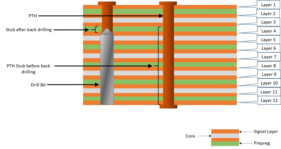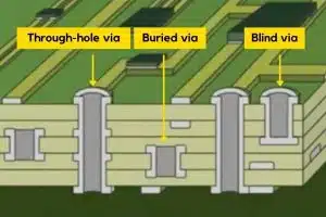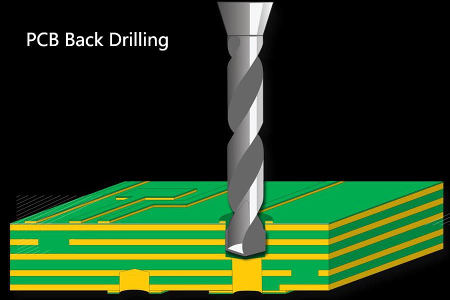
Backdrilled vias are a special type of plated through-hole vias that have the lower portion of the via “drilled away” after the PCB fabrication process.
As shown in the diagram below, they look like a normal via from the top of the PCB. However, the lower half of the via barrel is removed, leaving only the connections to the necessary inner layers.
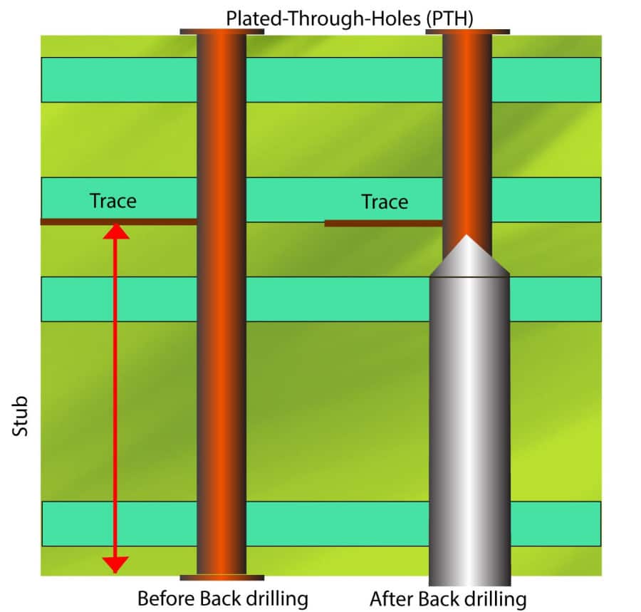
Plated through hole before and after back drilling
This contrasts with a regular via that spans the entire length from the top to the bottom layer, connecting all layers in between.
So why go through the extra fabrication steps to create these partial vias?
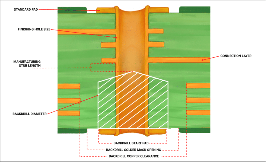
The answer lies in the inherent functionality of vias. As critical interconnects in multi-layer PCB boards, all vias exhibit an unavoidable parasitic effect at high frequencies known as the “via stub”. This disrupts clean signal transmission and propagation.
Backdrilling eliminates the lower stub section that is often unnecessary for signal routing between the surface and first few layers. This minimizes unwanted reflections and impedances that degrade signal integrity at high speeds.
In essence, backdrilled vias remove only the non-functional via length while retaining electrical connections between the necessary inner layer traces. This makes them ideal for high-density PCBs that require pristine signal transmission up to microwave frequencies.