What are pads in PCBs and why are they so important for electronics design and manufacturing? This definitive guide covers pad types, layout considerations, and the overarching significance of PCB pads.
Table of Contents
Introduction
Printed circuit boards serve as the foundation for electronics. They provide the interconnections between various components in a circuit. Pads are a critical part of the PCB design, enabling both the mounting and electrical connectivity of components. This article will provide an in-depth explainer on what PCB pads are and their significance in board design.
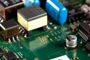
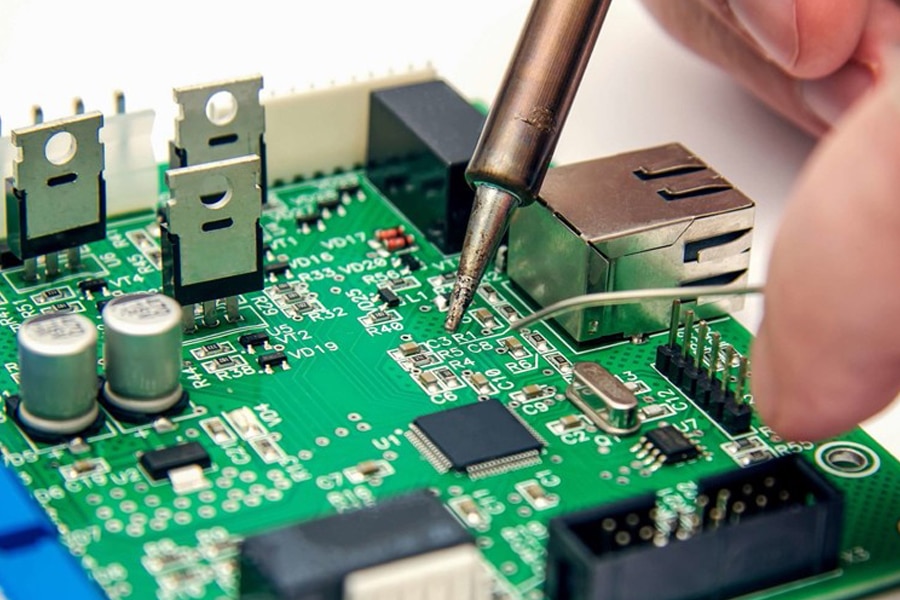
A pad refers to the metallic surface on the PCB circuit board where components are soldered and mounted. Pads allow components to be affixed to the board through soldering and form electrical connections via copper traces. The size, shape, and placement of pads heavily influence overall manufacturing quality and device reliability.
There are several types of pads used in PCB design, categorized by shape and functionality to suit various components and assembly requirements:
Shapes
Rectangular pads: Standard quadrilaterals for leaded components
Round pads: Circular shapes often used for through hole parts
Island pads: Isolated copper regions for surface mount IC contacts
Polygonal pads: Custom shapes with multiple straight sides
Oval pads: Elliptical pads used for some connectors
Cutout/Void pads: Pads with internal openings to allow venting
Specialty Pads:
Daisy chain pads: Interlinked flower-shaped pads
Cross-shaped pads: Self-centering cruciform test points
Teardrop pads: Rounded edge pads to avoid solder bridging
Functions:
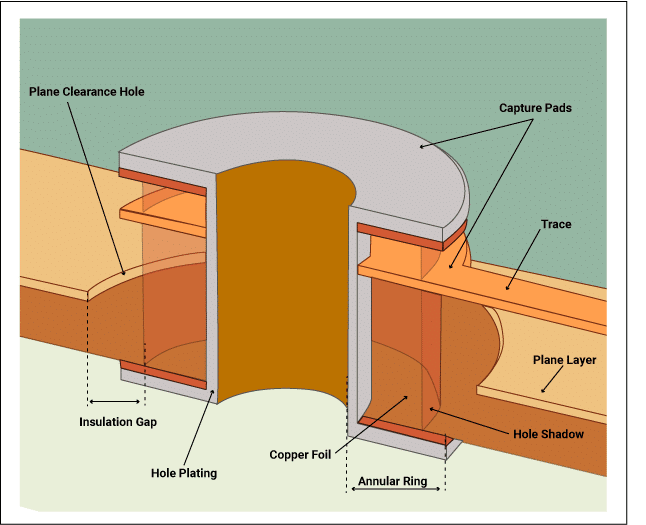
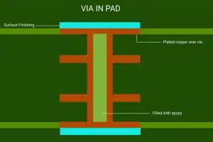
Through-Hole Pads: These are cylindrical pads that allow component leads to pass through the entire circuit board. The leads are then soldered onto the pad to form both a physical and electrical connection. As per IPC-2221 standards, typical annular ring dimensions range from 1.2mm to 2mm for these pads. Through-hole pads accommodate many leaded components like resistors, capacitors, and connectors.
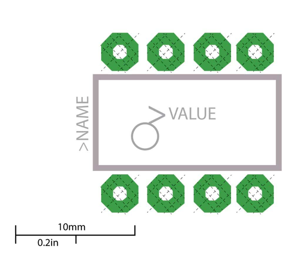
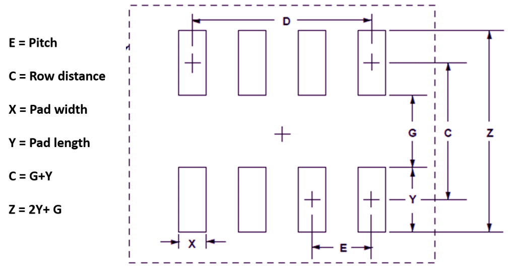
Surface Mount Pads: As components became smaller, surface mount technology emerged. This required flat copper pads on the board surface to mount devices. SMT pads have specially controlled dimensions and solder masks to enable reliable solder joint formation during reflow soldering. Common SMT components supported include chips, LEDs, and various integrated circuits with gull wing or J leads.
Thermal Pads: High power devices require heatsinking to prevent overheating. This is achieved by thermal pads connected to large internal copper planes. The pad area is proportional to the amount of heat that must be conducted away. Thermal vias help transfer this heat to inner or bottom copper layers. Common devices needing thermal pads include power amplifiers, motor drivers, and microcontrollers.
Test Points: Test points provide easy access to key nets on a board for validation and troubleshooting. They consist of through-hole or SMT pads connected traces that serve as test nodes. Minimal drilling is required compared to full poke-through holes. Test points help accelerate prototyping and failure analysis.
At JHYPCB, our advanced PCB manufacturing capabilities allow reliably fabrication of all pad varieties, from standard through-hole to intricate SMT and thermal pads. Our precision machinery and rigorous quality control ensure consistency across pad dimensions and locations.
Pad design for through-hole pads
Role of Pads in PCB Layout
The layout of pads on a printed circuit board holds critical importance from both design and manufacturing perspectives. Some key roles pads play in the board layout process includes:
Facilitating Component Placement: PCB designer begins by strategically placing components based on parameters like desired circuit topology, high-speed paths, heat dissipation needs etc. The footprints for components contain the pads. So pad layout mirrors component layout to enable mounting. Design rules help maintain adequate spacing between pads.
Enabling Trace Routing: Pads represent termination points allowing traces to interconnect different components placed across the board. Traces must correctly route signals between relevant pads based on schematics. Careful pad positioning reduces need for longer traces and minimizes crosstalk.
Accommodating Via Transitions: Vias help transition traces between layers. Their barrels must fully overlap with clearance around pads to avoid shorts. So pads locations must account for any planned via transitions nearby. This ensures reliable interlayer connectivity.
Allowing Board Assembly: The dimensions and tolerance of pads directly affects solder paste application, component placement, and ease of soldering during assembly stages. Optimized pad designs help maximize finished product yield and long term reliability.
At JHYPCB, years of PCB fabrication knowledge allow us to provide layout recommendations regarding pad arrangements tailored to customer requirements. Our capabilities also guarantee high consistency pads meeting stated specifications.
Pad design for surface mount pad
Significance of Pads in PCBs
Pads are one of the most vital elements in printed circuit board design. They enable both the structural mounting and electrical connectivity of almost all discrete components and integrated circuits. Some key reasons why pads hold such tremendous significance include:
Electrical Functionality: Pads connect components to the conductive copper traces on a PCB. This allows signals and power to propagate between different parts of the circuit network. Optimally designed pads are crucial for reliable performance.
Mechanical Stability: The soldered joints formed between component leads and pads provide a robust mechanical fixture. This allows the devices to securely reside on the board despite vibration or shock exposure.
Thermal Management: Pads provide the thermal interface enabling heat conduction away from hot devices into the board’s ground planes. Enlarged thermal pads on power devices are vital for effective heat dissipation.
Manufacturability: Dimensional accuracy and precision in pad size, shape and location directly impacts solder paste application, machine placeability, and ease of assembly. Well-designed pads enhance manufacturability.
In summary, PCB pads enable function, provide mechanical stability, facilitates cooling, and eases manufacturing for electronics components. At JHYPCB, we provide advanced fabrication capabilities allowing customers to harness the full potential of optimized pad implementations.
Conclusion
Pads are a small but extremely vital piece of the overall PCB architecture, enabling both the structural and electrical integration of components. Optimizing pad design and layout is crucial for achieving assembly success as well as long-term reliability of electronic devices.
This article provided an in-depth explainer covering fundamental pad types, layout considerations, and their overarching significance. Key takeaways include:
– Pads serve as soldered interface between component pins and PCB traces – Various pad shapes exist to accommodate through-hole and SMT parts – Pad size, positioning and spacing impacts manufacturability – Electrically, pads propagate signals and power within the circuit – Mechanically, pads ensure components stay fixed to board surface
At JHYPCB, we are committed to fabricating boards with consistently high-quality and dimensionally accurate pads per customer specifications, enabling your designs to achieve functional objectives. With nearly a decade of PCB manufacturing expertise, our streamlined prototyping to production capabilities powered over 10,000 customers globally. Contact us today to bring your electronics vision to reality.
JHYPCB is a leading PCB prototyping, PCB manufacturing and assembly service provider in China, offering quick turn PCB prototyping, multi-layer PCB manufacturing and turnkey PCB assembly services.