In the first sections, we walked through the initial PCB fabrication steps – milling the blank laminate, applying copper foil, and mechanically drilling holes. We then covered the copper electroplating process to deposit copper in the drilled holes and build up the thickness of the traces. Photolithography was also detailed, using UV light to transfer the layout pattern onto the copper layer. Areas unprotected by the photoresist are etched away, leaving only the desired conductive copper traces.
Now we have a layered PCB substrate with conductive traces and plated-through holes. In this next portion, we will focus on two additional major steps that complete the PCB production sequence – pattern plating and automated optical inspection (AOI). First, we will explain the photoresist stripping process which removes the remaining protective photoresist material after etching. This fully exposes the copper traces for component soldering. Finally, automated optical inspection utilizes high resolution cameras to verify the quality and accuracy of the fabricated board by comparing it to the original PCB design files. With AOI validation, the PCB is finished and ready for electronics assembly and soldering.
Step 5: Pattern Plating
Pattern plating, also known as photolithographic plating, consists of several key stages: copper plating, tin plating, resist stripping, etching, and tin stripping. All these steps rely on chemical reactions.
Copper and Tin Plating
After the routing process, the circuit board is first sent to the pattern plating production line to complete copper and tin plating.
At this point, copper is exposed along the traced pathways while the untraced areas remain covered by protective resist. Copper plating deposits an additional layer of copper, thickening the existing copper traces and plated-through holes. The resist film blocks copper deposition on the untraced areas.
Tin plating follows to apply a thin layer of liquid tin onto the copper traces. This transient tin layer serves to protect the copper during subsequent resist stripping by preventing copper oxidation and etching. The sacrificial tin layer is eventually removed in the final stage of the pattern plating process.
As shown in Figure 5-1, mid-production boards move along the pattern plating line. The top row shows boards before plating with exposed copper traces. The bottom row displays completed boards after copper and tin plating, evident from the white tin coating on all copper traces. The untraced laminate areas show different tinted colors under lighting, ranging from blue to black to purple, depending on the resist properties.
Resist Stripping, Etching, and Tin Stripping
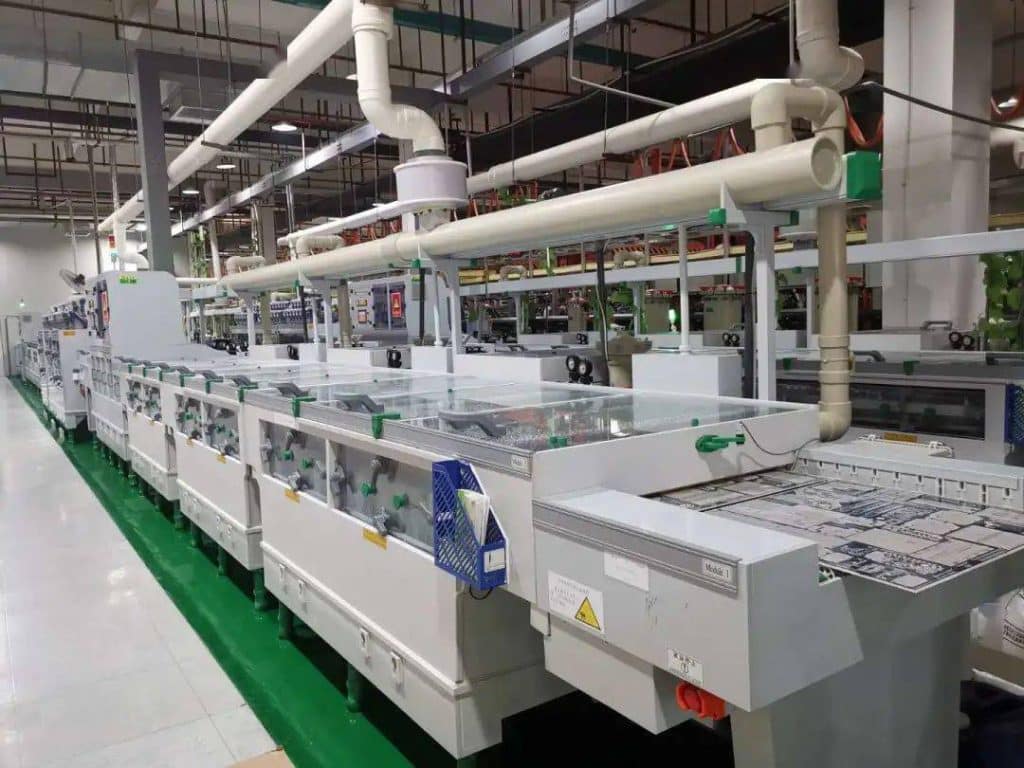
After copper and tin plating, the boards enter an automated production line for resist stripping, etching, and tin stripping, shown in Figure 5-2. A board can be seen entering the line, going through resist stripping first. The stripping agent reacts only with the UV exposed resist, completely removing it after two rinse cycles.
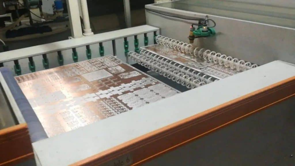
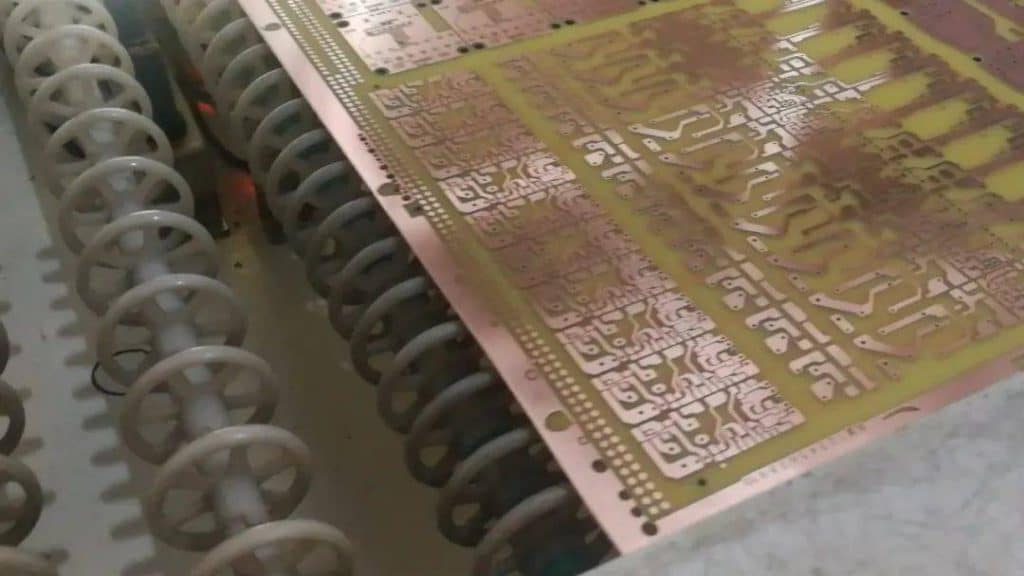
As shown in Figure 5-3, this circuit board has completed resist stripping. The protective resist film is now gone, exposing the blank copper laminate in those regions. However, the desired copper traces remain protected underneath the plated tin layer.
Next is the crucial etching step, where the board proceeds into etching solution baths. The etchant liquid erodes and dissolves the now exposed copper surfaces on the untraced areas. This effectively removes all the unwanted blank copper, while the tin coating shields the intended conductive copper traces from being etched away.
The etching stage utilizes an etchant solution that selectively reacts with copper but not tin. As the boards convey through the etching baths, the exposed blank copper laminate that was uncovered after resist stripping gets progressively dissolved away. However, the intended copper traces remain protected under the transitional tin plating.
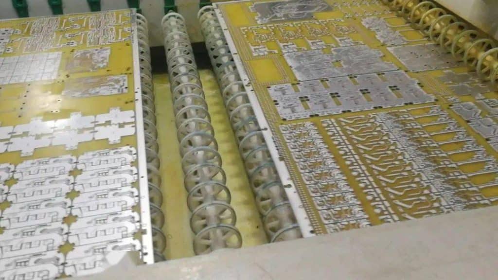
As shown in Figure 5-4, the traces appear white, indicating the tin coating persists through etching without any reaction. This allows the underlying copper traces to remain intact. Meanwhile, the previously exposed blank copper surfaces have been removed by the etchant, revealing the bare substrate underneath.
After etching, only the desired conductive copper pathways are left on the laminate, still shielded by the plated tin layer. This tin coating is later chemically stripped off, leaving a printed circuit board with defined copper circuitry ready for component assembly and soldering.
The boards proceed downwards on the conveyor into the tin stripping stage. This step utilizes a chemical solution that selectively reacts with tin, completely removing the transitional plating from the copper traces.
As shown in Figure 5-5, the resulting boards have finished tin stripping. The protective immersion tin coating applied during the plating process has been stripped away. This exposes the copper circuitry – traces, pads, and vias – in their final form, ready for component assembly and soldering.
The pattern plating sequence involving copper plating, tin plating, resist stripping, etching, and tin stripping transforms the laminate into a functional printed circuit board. The end result is a PCB with defined copper pathways that will serve as conduction channels for surface-mount components to be soldered on.
The fabricated boards proceed on roller conveyors into the automated optical inspection (AOI) system, as shown in Figure 5-6. Four high-resolution cameras mounted above the conveyor perform a scanning image capture of the entire board. This prepares the board for subsequent AOI analysis.
The AOI software then imports these images and essentially compares the physical board against the original PCB design files. It utilizes advanced pattern recognition and computer vision algorithms to precisely identify any defects, abnormalities, or quality issues with the fabricated circuitry. For example, opens, shorts, spacing violations, missing copper, misregistration, and more.
Any boards that fail this automated optical validation get flagged for manual inspection, rework, and rectification. Only boards that pass AOI reach the next production stages. This inspection, repair, and verification loop helps ensure consistent quality and reliability of the finished PCB production.

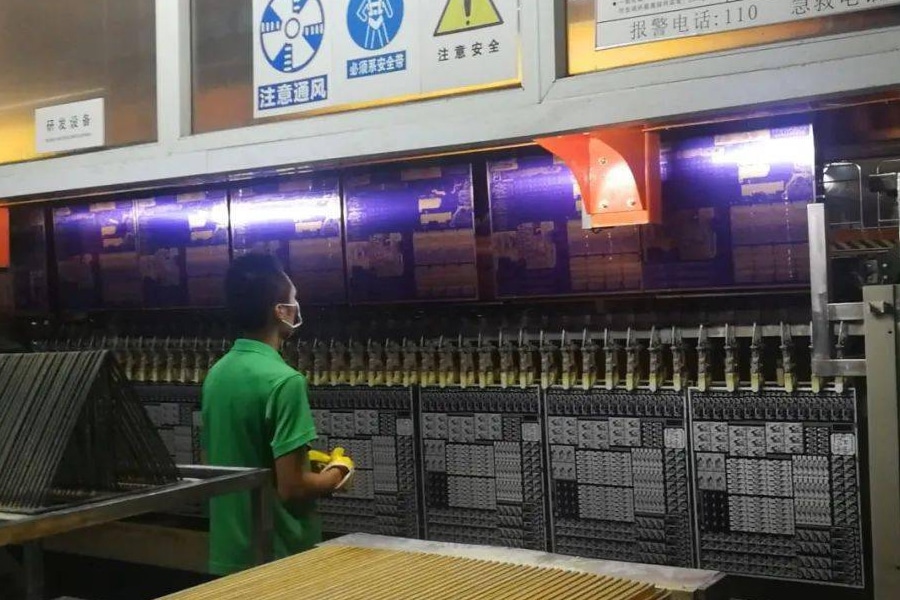
Step 6: AOI
AOI stands for Automated Optical Inspection. As shown in Figure 6-1, operators at JHYPCB are performing AOI on printed circuit boards immediately after pattern plating.
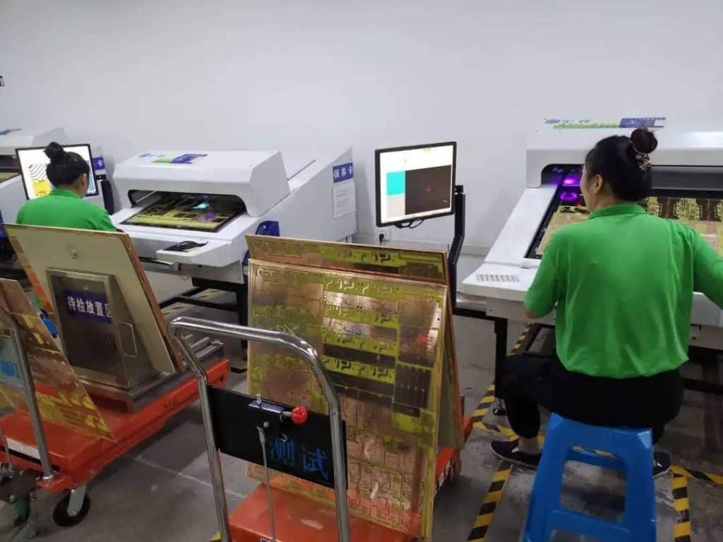
The AOI inspection principle is as follows: The PCB to be tested is placed on the AOI machine stage. The AOI scanner automatically captures images of the entire board, comparing them to the original design files from CAM. Any differences detected will stop the process, enlarge and display the discrepancy area to monitors.
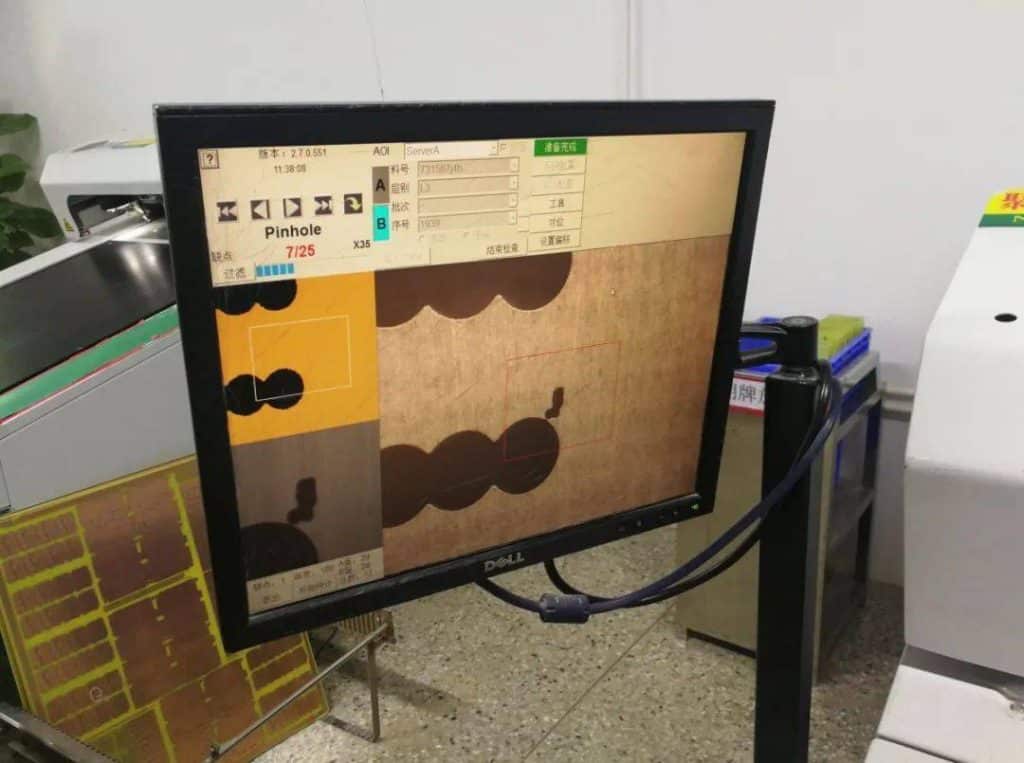
As shown in Figure 6-2, there are three images. Top left is the PCB layout from design. Bottom left shows the detected defect location against design. The enlarged right image presents the surrounding region of the defect for easy observation.
Operators visually inspect the flagged regions to confirm if they are actual defects. If verified to be false calls, inspection continues to the next location. For confirmed defects, they assess if rework is possible. Reworkable defects are repaired, while irreparable ones are logged as production defects, marking the fault site.
AOI scanning focuses only on inspecting PCB external visuals, excelling at detecting opens, shorts, broken traces etc. However, it cannot validate if all plated through-holes are properly conductive – that verification happens later in flying probe or fixture testing.
At this point, the AOI process is finished. Boards move to the next step: solder masking.
In the next article, we will learn about solder mask application, silkscreen printing, and hot air solder leveling.


