sales@pcbjhy.com

Sales Manager: Ms. Megan

+86-13825274100

24/7 Customer Support

+86-13825274100

WeChat and WhatsApp

What are Tented Vias? A Guide to This Important PCB Feature

What are tented vias and why should PCB designers use them? Read our full guide covering how tented vias work, their benefits, ideal applications, and how to construct boards with quality via tenting.
Tented Vias in PCB Board

Table of Contents

What is a Tented Via?

If you deal with PCB design or manufacturing, you have likely encountered various types of plated-through holes called vias used to interconnect layers and components. From standard through-hole vias to blind vias and buried vias, these metal-plated holes enable signals, power, and ground to traverse across multiple PCB layers.

Now you may come across another special variety – the so-called “tented via.” As the name suggests, tented vias have a “tent” or protective cover on one or both ends of the hole. But what exactly are they and what purpose does tenting a via serve for your PCB?

In this definitive guide, we’ll cover everything you need to know about tented vias including:

  • What is a tented via in a PCB?
  • Key reasons PCB designers use tented vias
  • How do tented vias differ from PTHs, blind vias, buried vias, and microvias?
  • Construction, design considerations, and limitations

Whether you are just learning PCB design concepts or are a veteran, read on to gain an in-depth understanding of tented vias in printed circuit boards. Or, if you’re ready to order PCBs with high-quality tented vias fabricates accurately to your specifications, contact our expert team at JHYPCB.

What is a Tented Via in PCBs?

A tented via is a plated through-hole or PTH in a printed circuit board which has been deliberately covered or “tented” with solder mask on the top side, bottom side, or both sides of the board. This solder mask tenting material encapsulates the via, leaving just the barrel exposed within the PCB layers, but covers up the actual hole openings.

In contrast, standard unfabricated PCBs often have all of their vias fully exposed on both sides. The application of a thin layer of soldermask over one or both ends of a via allows it to become “tented” as the mask forms a protective barrier or tent. Tents are usually 10-30 microns thick.

There are a two main types:

  • One-sided tenting: Via opening is covered on only one side of the PCB, either the top or bottom. The other end remains open.
  • Two-sided tenting: The via hole is fully encapsulated, with soldermask applied on both sides of the board during fabrication. This fully seals the via.

In a sense, the soldermask tenting material provides a “roof” over the via hole. This tents them in the same way a waterproof canvas provides shelter. We’ll explore why this tenting is useful next.

Tented Vias Types

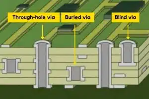
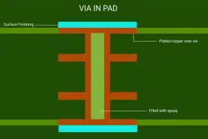
IPC-4761 Type I: Tented Via
The via is covered with a stretched Dry film solder mask without any additional materials.

Tented Vias Types - One Sided - Type 1-a

Tented Vias Types – One-Sided – Type 1-a

Tented Vias Types - Double Sided - Type 1-b

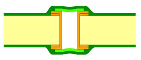
Tented Vias Types – Double Sided – Type 1-b

IPC-4762 Type II: Tented & Covered Via
The entire via has been coated with a layer of dry film solder mask. Then a layer of regular solder mask was printed on top of it.

Tented Vias Types - One Sided - Type 2-a

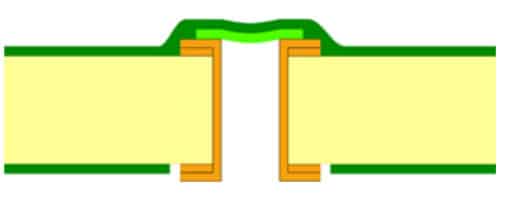
Tented Vias Types – One-Sided – Type 2-a

Tented Vias Types - Double Sided - Type 2-b

Tented Vias Types – Double Sided – Type 2-b

Why Use Tented Vias in PCB Design?

Tented vias offer some clear benefits compared to exposed, untented vias:

  • Improved Insulation
    Covering via holes eliminates air gaps around the barrel hole which could potentially cause arcing or signal leakage between layers, especially in high density, high frequency designs. The soldermask “tent” provides a protective barrier and enhanced insulation properties.
  • Prevents Solder
    Wicking and Drips Exposed vias allow solder to wick down into the via hole during reflow soldering. This can create an unsightly mess and risks bridging contacts if excess drips out. With tented vias, the soldermask cover prevents this wicking action, keeping solder where it is intended.
  • Allows Routing Traces Over Vias
    In complex, dense PCBs, design may require routing thin circuit traces directly over via locations. A tented via provides necessary insulation when traces must crossover its hole. This enables greater flexibility with layouts.

Let’s go on to explore the PCB applications where tented vias offer the most benefit to designers.

When Should Tented Vias Be Used?

There are certain PCB design situations where implementing tented/covered vias pays dividends:

  1. High-Density Components Both Sides
    With components and circuitry on both sides of the board, tenting via holes prevents solder trails down the holes which could cause shorts. This makes tented vias well-suited for dense double-sided boards.
  2. Signal or Plane Layers Above Vias
    In complex multilayer boards with signal routing and plane layers above vias, the tented layer gives insulation allowing traces to safely pass over underlying vias. Two-sided tenting gives maximum insulation.
  3. When Clean Visual Aesthetics Matter
    For consumer products where look and perceived quality are important, nicely tented vias prevent unsightly solder drips and delivers visually cleaner results. Their uniform appearance also aids inspectability.
  4. EMI/EMC Shielding Needed
    Fully enclosed tented vias help meet rigorous electromagnetic interference (EMI) and compatibility requirements by blocking interference leaking through open holes between layers.

Next we’ll examine exactly how printed circuit board manufacturers construct these tented via holes during fabrication.

How Are Tented Vias Constructed?

During the PCB fabrication process, tented vias are constructed using soldermask, either through:

Mask Tenting – Small areas of soldermask are retained over both via holes during the standard PCB masking process. This single step masks the vias along with the rest of the board.

Paste Tenting – Via holes are first left uncovered through the fabrication sequence. Then after all other soldermask steps, an extra tenting paste is printed specifically to cover just the exposed via holes as a second step.

Both methods result in the same tenting effect of encapsulating the vias in insulating soldermask. Paste tenting allows vias to be initially left uncovered for any plating or filling steps if required.

For one-sided tenting, soldermask is only left or applied over vias on either the top or bottom side. Two-sided tenting fully seals both sides.

The thickness of the dry soldermask layer is typically 0.01 to 0.03mm (10 – 30 microns), allowing a measure of insulation and resistance to solder wicking, but avoiding excessive material which is difficult to fully cure during lamination.

Next we’ll look at some special considerations PCB designers should keep in mind when working with tented vias.

Tented Via Design Considerations

While tented vias provide advantages, engineers should keep the following guidelines in mind:

  • Ensure vias are properly filled to avoid potential air gaps under tents which undermine insulation performance. Common fills include conductive materials like copper or non-conductive epoxy paste.
  • Account for some increase in thermal resistance. The tented layer slightly inhibits heat conduction away from components through the via barrel. This requires attention to thermal design constraints.
  • With two-sided tenting, allow adequate ventilation, airflow and heat sinks to avoid excessive component heating, especially around heat-sensitive parts.
  • Use a reputable PCB manufacturer who demonstrates consistent quality tenting and properly fills vias to specification. Verify their capabilities before ordering.
  • Work with your board house/supplier if tentative tests reveal issues with tents lifting during soldering or inspection processes.

While tented vias require special construction care, an experienced fabricator like JHYPCB ensures your finished boards realize the full benefits of tenting without reliability issues.

Next we wrap up with a summary of when tented vias play an invaluable role.

Leveraging the Benefits of Tented Vias

As we’ve covered in this guide, tented or covered vias provide clear advantages compared to exposed plated through-holes in complex printed circuit board designs:

  • Enhanced insulation between layers when routing high density traces
  • Avoiding solder-wicking aesthetics issues
  • Allowing crossover routing over via locations
  • Noise isolation and EMI/EMC shielding

Advanced PCBs integrating high speed signals, intricate component layouts, and rigorous quality demands can benefit greatly from specifying tented vias.

However, realize tenting does present some fabrication and design considerations around filling, ventilation and inspection testing. Working closely with your board house is key to success.

With over 15 years of experience delivering quality PCBs, JHYPCB has the technical PCB fabrication expertise to construct boards with reliable tented vias built exactly to your specifications the first time. Contact us for more information or submit your design files for an instant quote.

Related Reading

About Me

JHYPCB is a leading PCB prototyping, PCB manufacturing and assembly service provider in China, offering quick turn PCB prototyping, multi-layer PCB manufacturing and turnkey PCB assembly services.

Recent Posts

PCB assembly service
Scroll to Top