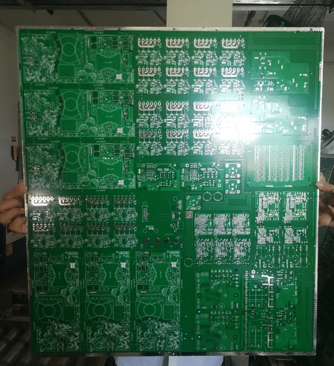
So far, we have covered the initial foundations of PCB fabrication – substrate preparation, drilling, copper plating, photolithographic patterning to form the conductive circuitry, and optical inspection to verify board quality. We now move to the next set of enhancements in the manufacturing sequence.
In this section, we will detail three important steps – solder masking, silkscreen printing, and surface finishing. First, we will explain solder mask application which coats the entire board except the solder pads to prevent short circuits. Next is legend printing to add informative labels, logos, and markings using the silkscreen method. Finally, we will describe surface metal treatments like ENIG and immersion tin that protect pad corrosion and improve solderability.
With the addition of these aesthetic and functional processes, the PCB further progresses towards assembly readiness. Note this is still not the end of the fabrication workflow. Subsequent articles will cover final stages like electrical testing, quality assurance, and shipment preparation. For now, we focus on key enhancement and protection steps that ready the quality-inspected board for population.
Step 7: Solder Mask
After previous processes, the PCB is now a semi-finished product. The next step is solder masking.
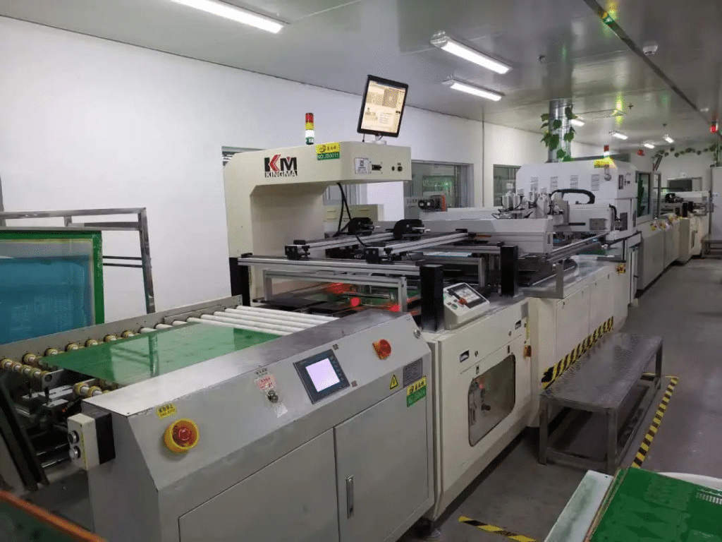
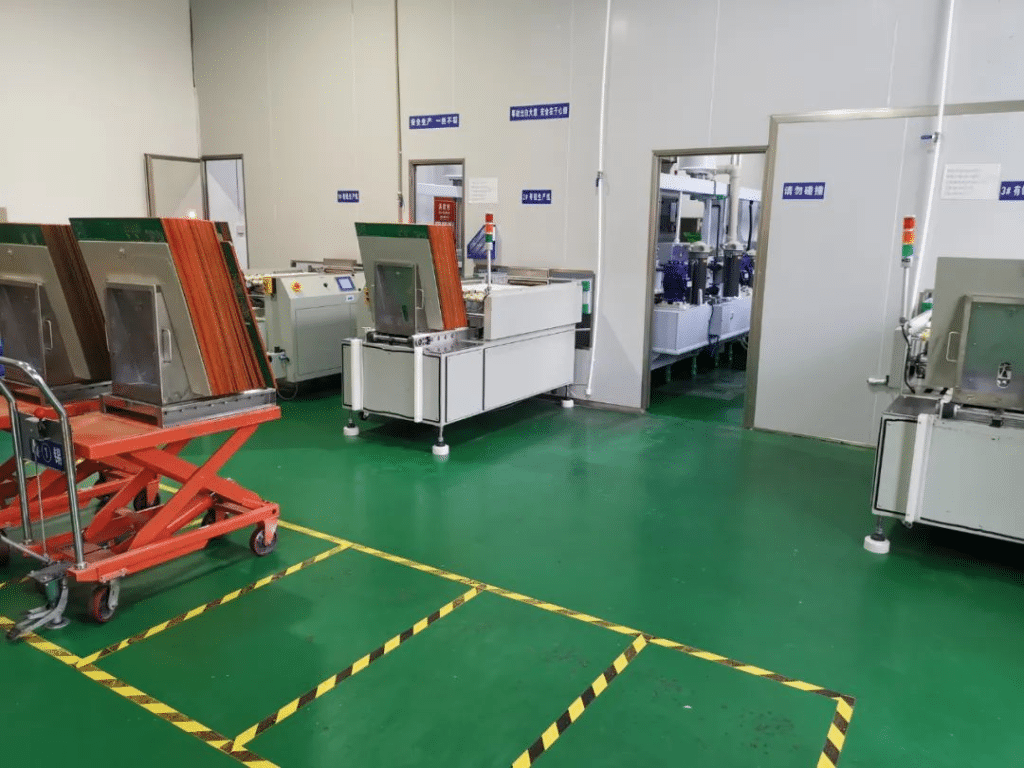
As shown in Figure 7-1, this is a solder mask printing line at JHYPCB. Boards waiting for masking on the left reveal exposed copper traces.
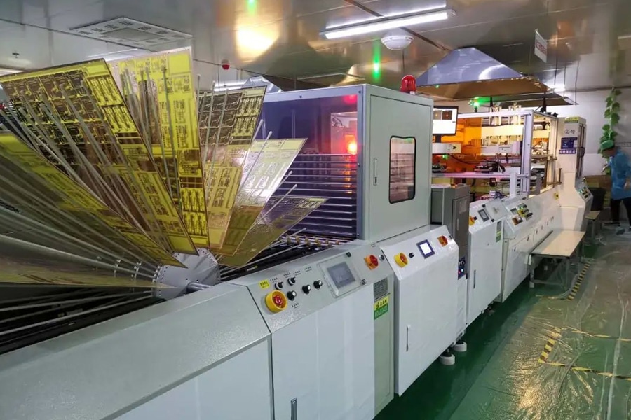
The exposed copper traces are susceptible to oxidation when interacting with air. Copper oxide formation impairs board performance over time and reduces PCB lifespan. This is where solder masking in the next step plays a crucial role.
The purpose of solder mask application is to coat the entire board surface with a protective polymer layer that shields the copper from corrosion. The most common color is green, but blue, black, white, red, yellow, purple options are also available. JHYPCB currently provides all solder mask color variants free of charge.
The solder masking process closely resembles the earlier photolithographic patterning sequence. Just like the imaging, exposure and development steps used during routing, solder mask application also involves printing the mask material, exposing it under UV light, and finally developing to remove unpolymerized areas.
Solder Mask Printing
Prior to solder mask printing, the boards undergo several pretreatments – acid cleaning, surface abrasion, multi-stage rinsing etc. These steps utilize chemical reactions. After waiting exposed for a period, the copper traces have likely oxidized slightly in air. So acid cleaning first removes this copper oxide and other contaminants like oils. Abrasion then roughens the laminate to improve photoresist adhesion.
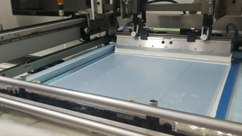
As shown in Figure 7-2, this solder mask printer has a patterned screen to apply green liquid photoresist (LPI) onto boards. A PCB after pretreatments has auto-loaded under the screening frame.
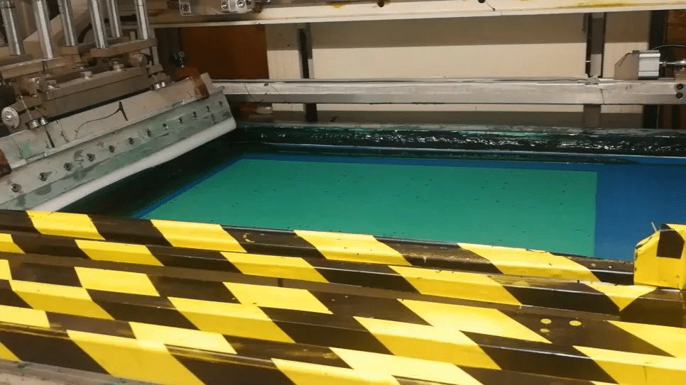
After screening through the solder mask printer, a layer of green liquid photoimageable resist covers one side of the PCB. The board proceeds into a flipper mechanism that inverts it before entering the second printer for applying resist onto the other side. Now both sides are coated with green solder mask material.
The boards then convey through a series of high temperature ovens set at precise preprogrammed profiles. Over a period, the heat exposure partially cures the liquid resist, transforming it into a protective dry film coating that adheres firmly to the PCB.
Exposure
The previous step indiscriminately coated the entire board surface with solder mask on both sides, including areas like solder pads that should remain uncoated. To selectively remove resist material from these regions, the boards now undergo exposure and development.
As depicted in Figure 7-3, this is an automated solder mask exposure line at JHYPCB. Boards waiting in queue for imaging are seen on the left.
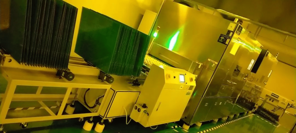
Exposure utilizes solder mask phototools where regions needing openings like solder pads are rendered opaque in black, while surrounding areas are fully transparent. When boards coated with liquid resist pass under these phototools, UV only reaches the transparent non-pad sections. The underlying resist in these regions receives full exposure while mask over pads remains unexposed, forming the exposure pattern required for subsequent developing.
Development
Similar to previous photolithographic steps, development relies on a chemical process where the developer solution only reacts with the unexposed areas of the resist film. As boards convey through the developing baths, the liquid mask coating over solder pads and other regions blocked from UV gets dissolved away, baring the underlying copper.
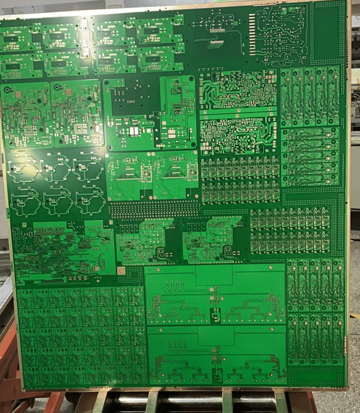
As shown in Figure 7-4, boards after development have exposed copper-colored solder pads, while the surrounding laminate remains protected under the hardened green solder mask. The sequence of printing, imaging, and developing transforms the blank PCB into a professionally solder-masked board ready for component assembly.
Step 8: Legend Printing
Legend printing adds top overlay graphics like component designators, outlines etc originally drawn in the PCB silkscreen layer. White ink is typically used, or black on white boards.
JHYPCB employs two legend printing methods – traditional silkscreen printers and laser-based systems.
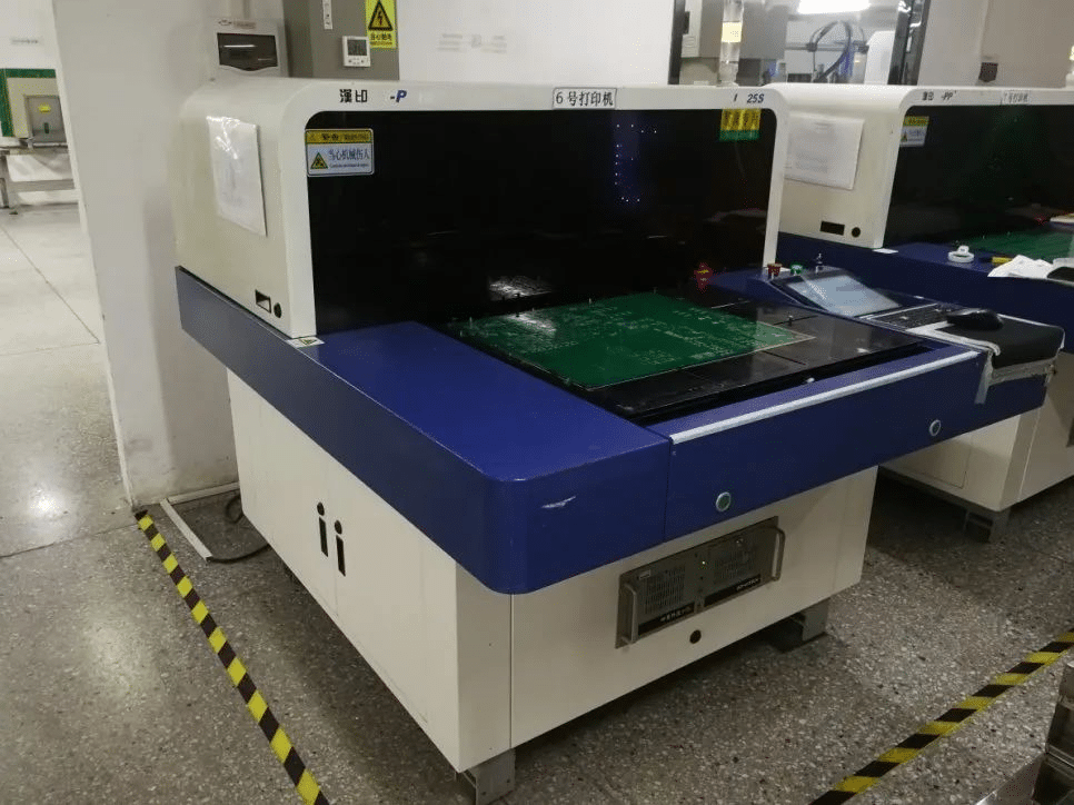
As shown in Figure 8-1, this fully automated legend printing line has two silkscreen printers for the top and bottom sides of a PCB.
As shown in Figure 8-2, the silkscreen printer is applying white ink onto a PCB. A white patterned screen is observed, which transfers ink only in desired areas. Similar screen materials are used for both solder masking and legend printing. But unlike the previous solid green solder mask screens, legend screens only transfer ink through open areas with actual printed graphics.
Similarly, double-sided printing is required to add legends on both top and bottom. Printed boards then bake in high temperature ovens to properly cure the ink and cement adhesion.
As shown in Figure 8-3, laser-based legend printers directly image the overlay layers without screens. They output sharper motives at lower speeds compared to traditional screen printing. Laser systems are well-suited for prototyping while high volume production utilizes conventional stenciling.
Step 9: Surface Finishing
After legend printing, surface metal treatments are applied to enhance solder pad solderability and protect against oxidation. This step is also known as surface finishing among PCB experts.
When ordering from JHYPCB, customers can choose immersion tin or ENIG (electroless nickel immersion gold) surface finishes for their boards. Tinning deposits a silver tin alloy while ENIG coats pads with a gold layer instead.
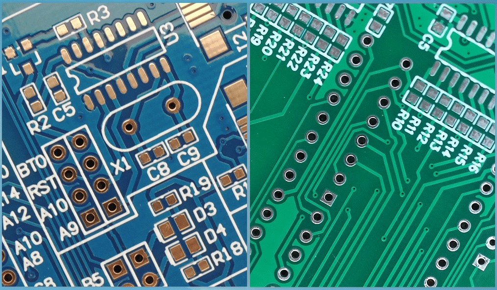
As illustrated in Figure 9-1, plated gold ENIG pads are on the left versus tinned copper on the right after immersion tinning.
Regardless of finish, surface treatments aim to serve two key functions – preventing copper oxidation, and improving solderability for component attachment.
The immersion tinning process consists of three main steps – pretreatment, hot air solder leveling, and post-treatment.
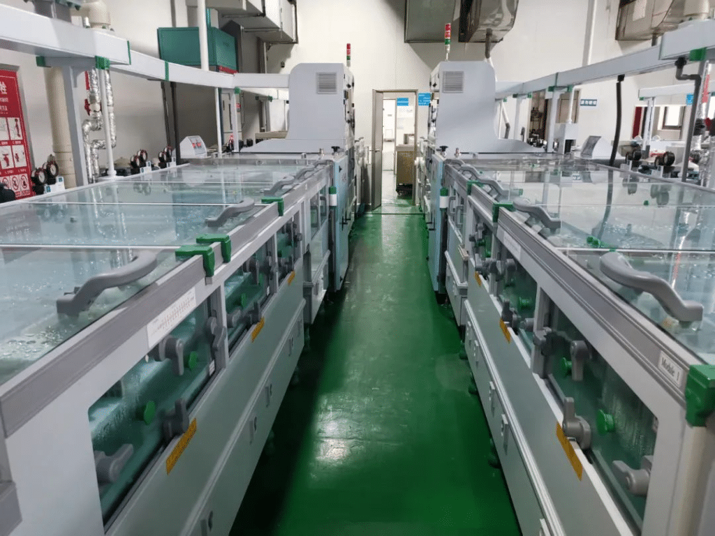
As shown in Figure 9-2, this is the tinning facility at JHYPCB. Boards can be seen loaded at the inlet of the pretreatment line.
As depicted in Figure 9-3, this is the pretreatment section boards first enter. Pretreatment involves microetching, abrasion, rinse cleaning, and rosin plating steps.
Microetching first removes surface contamination on boards. This is followed by rinse cleaning to flush off microetchant residues. Next, fine 1000 grit sanding belts lightly abrade the PCB. This removes minor surface deposits without damaging the laminate and traces. Another wash then preps for the subsequent rosin plating step, where boards are dipped in a flux bath to coat with this solderability agent.
(Tips – for sandpaper grit sizes, the higher the number, the finer the abrasive particles. Above 800 is considered extremely fine grinding.)
With pretreatment complete, hot air solder leveling can now be performed. Also called HAL tinning, Figure 9-4 shows the HAL machine at JHYPCB.
Boards dwell for seconds in the molten tin pot held between 230-250°C before exiting. They immediately pass under high velocity air knives which blow level the still liquid solder coating on pads and traces, smoothing it out while preventing blobbing. The previously yellowish copper surfaces now appear silver colored after tinning.
But this is not the end – post-treatments still remain. Figure 9-5 shows the post-tinning line at JHYPCB.
Post-processing primarily involves treatments such as hot water washing, plate grinding, cold plating, and drying. After the circuit board undergoes tin-spraying, it emerges from a tin furnace at a temperature exceeding 200 degrees Celsius, maintaining a high temperature. Initially, it traverses an air-floating bed—a typical assembly line that blows air from below, causing the circuit board to partially float in the air. This process resembles someone blowing on a freshly baked sweet potato to cool it down. Here, the air-floating bed serves the purpose of cooling.
Following the passage through the air-floating bed, a hot water wash is conducted. Why hot water? Because, at this stage, the circuit board’s temperature hasn’t completely decreased. Using cold water could lead to deformations and surface misting.
After the hot water wash, the board undergoes plate grinding to eliminate impurities like tin dross from its surface. Subsequently, it undergoes a rinse with clean water, followed by drying, marking the completion of the post-processing.
Once post-processing is finished, the circuit board’s surface is exceptionally clean, as depicted in Figure 9-6. This showcases the circuit board post the tin-spraying process.
At this point, the tin-spraying process is complete.
In the next article, which is also our final installment, we will cover testing, edge profiling, V-CUT, quality control (QC), and shipping.


